Chip fuse and its making method
A fuse and chip-type technology, applied in the manufacture of fuses, emergency protection devices, electrical components, etc., can solve the problems of thermal stress and protective layer damage, high manufacturing costs, etc.
- Summary
- Abstract
- Description
- Claims
- Application Information
AI Technical Summary
Problems solved by technology
Method used
Image
Examples
Embodiment Construction
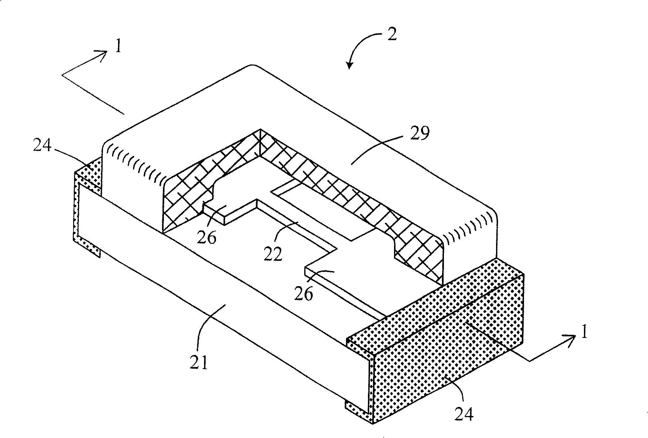
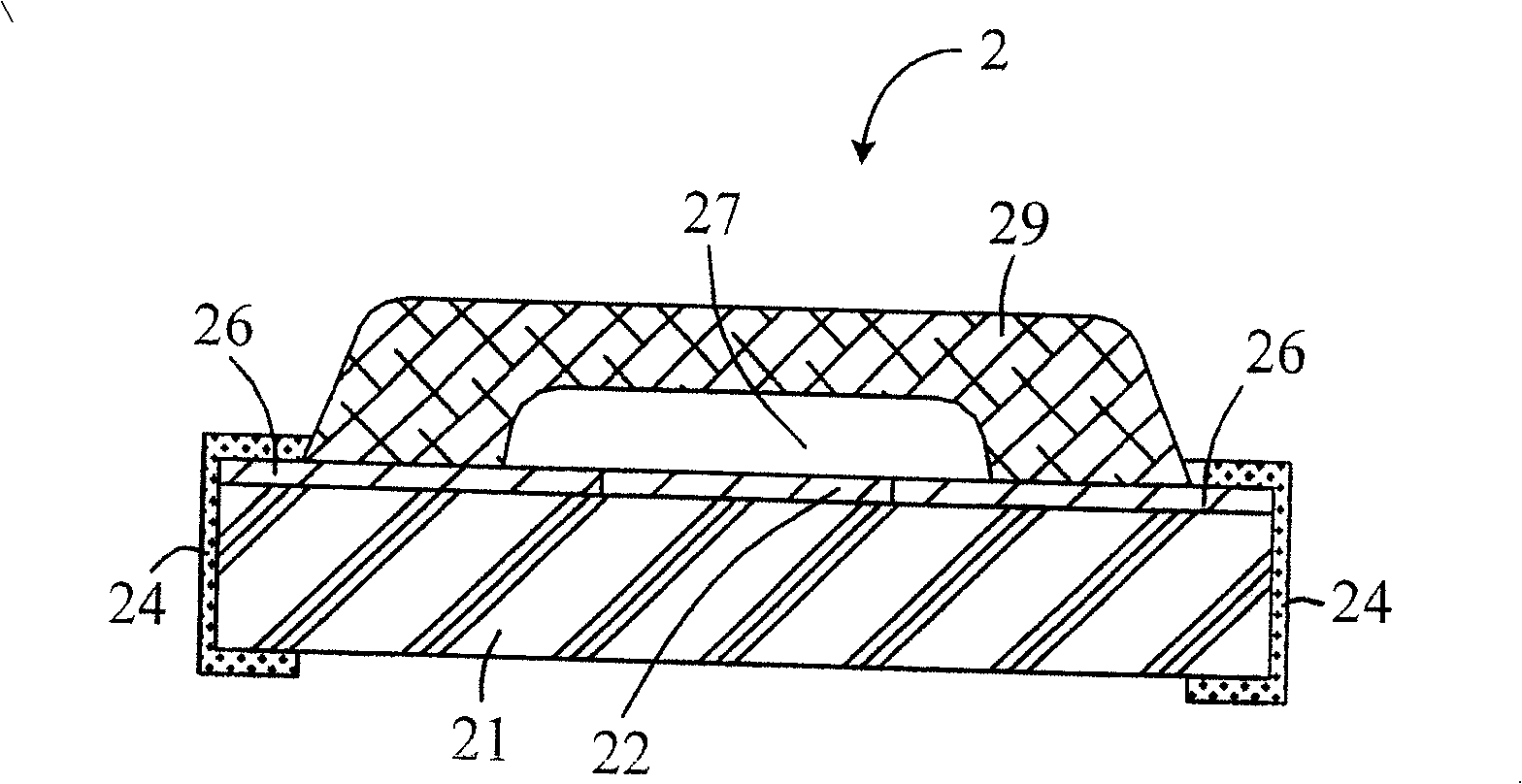
[0060] see figure 2 , figure 2 A perspective view of the chip fuse 2 according to the first preferred embodiment of the present invention is shown. The protective layer 29 is partially cut in the length direction and the width direction to clearly show the internal structure. image 3 for figure 2 Sectional view cut along the width centerline (1-1 line). The chip fuse 2 includes a substrate 21 , a fuse 22 , a cavity 27 , a protective layer 29 , two terminal electrodes 24 and two terminal pads 26 .
[0061] The substrate 21 is electrically insulating, and its material is alumina with a purity of more than 90%, glass, or other electrically insulating ceramic materials, wherein alumina with a purity of 96% is the most suitable, and its thickness is about 0.2 to 1.0 millimeters (mm).
[0062] Fuse 22 is a layer of conductive film, its composition is gold, silver, aluminum, copper, platinum and other pure metal or alloy, also can be silver and glass composite conductor, made...
PUM
| Property | Measurement | Unit |
|---|---|---|
| Width | aaaaa | aaaaa |
| Thickness | aaaaa | aaaaa |
Abstract
Description
Claims
Application Information


