Method and system for laser thermal processing of semiconductor devices

a laser thermal processing and semiconductor technology, applied in the field of laser thermal processing, can solve the problems of reducing the heat required to melt and activate the junction, the upper limit of the process window is restricted, and the poly-gate may deform and become incapable of performing the device's required function, so as to achieve the effect of preventing melting

Inactive Publication Date: 2005-01-18
VEECO INSTR
View PDF4 Cites 22 Cited by
  • Summary
  • Abstract
  • Description
  • Claims
  • Application Information

AI Technical Summary

Benefits of technology

An aspect of the invention is a system for performing LTP of a semiconductor structure that includes a substrate and a temperature-sensitive element, such as a poly-gate of a transistor. The system comprises a dielectric cap formed atop the temperature-sensitive element. An absorber layer is formed atop the substrate and the dielectric cap. The dielectric cap is adapted to insulate the temperature-sensitive element from heat transmitted by the absorber layer during LTP to prevent melting of the temperature-sensitive element. The dielectric cap may also be formed to substantially prevent implantation particles from reaching the temperature-sensitive element during an implantation process, e.g., an amorphization or dopant implant. A further aspect of the invention includes a switch layer formed atop the absorber layer. The switch layer is either a reflectivity-switch layer or a phase-switch layer.

Problems solved by technology

However, on certain types of device wafers, the upper limit of the process window is restricted by the possibility of melting select temperature-sensitive elements in the device.
After melting and recrystallization using LTP processing, the poly-gate may deform and become incapable of performing its required function in the device.
Unfortunately, in the prior art process and structure described above in connection with FIG. 1, the amount of heat required to melt and activate the junction is often very close to the amount of heat needed to melt a temperature-sensitive element such as a poly-gate.
This melting could deform the poly-gate, which typically ruins the device.

Method used


Image

  • Method and system for laser thermal processing of semiconductor devices
  • Method and system for laser thermal processing of semiconductor devices
  • Method and system for laser thermal processing of semiconductor devices

Examples


Embodiment Construction

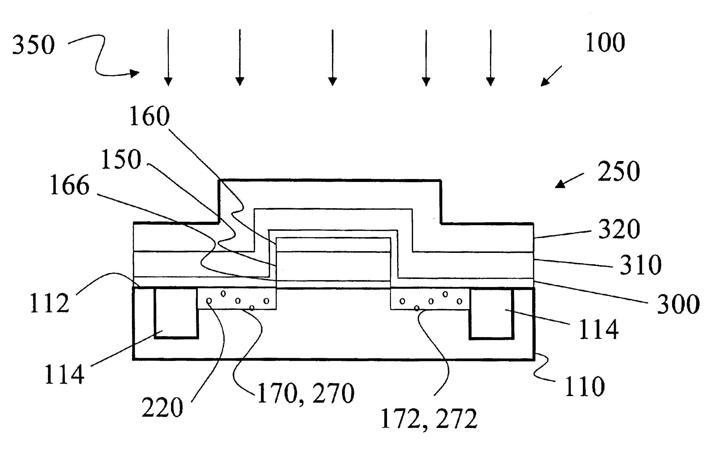
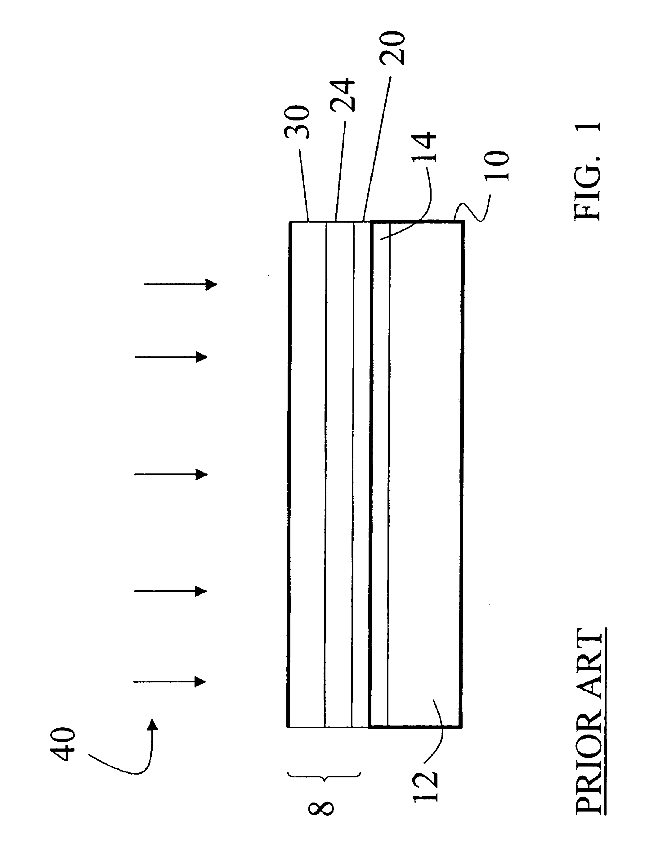
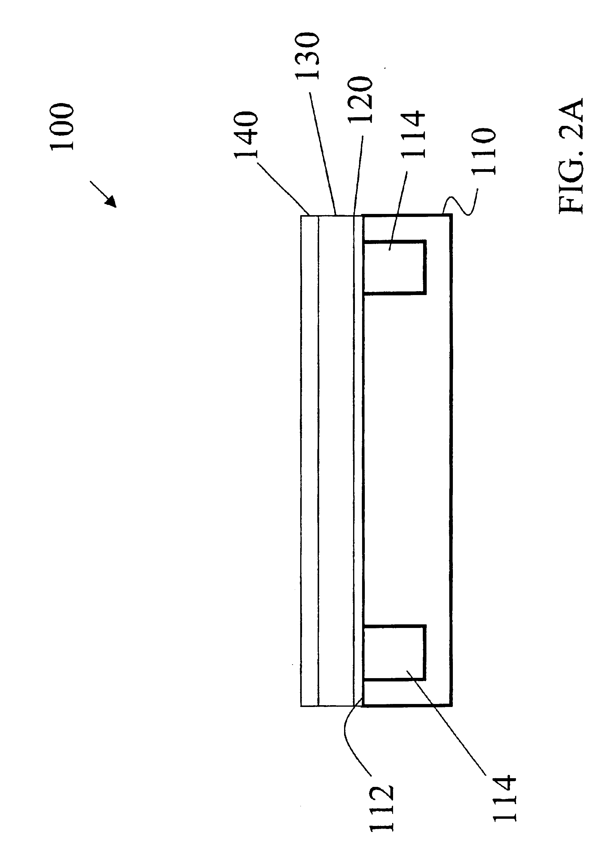
In the following detailed description of the invention, reference is made to the accompanying drawings, which form a part hereof, and in which is shown, by way of illustration, specific embodiments in which the invention may be practiced.

In the drawings, like numerals describe substantially similar components throughout the several views. The embodiments are described in sufficient detail to enable those skilled in the art to practice the invention. Other embodiments may be utilized, and structural or processes changes may be made without departing from the scope of the present invention.

The terms wafer and substrate used in the following description include any structure having an exposed surface with which to form the integrated circuit (IC) structure of the invention. The term substrate is understood to include semiconductor wafers. Both wafer and substrate include doped and undoped semiconductors, epitaxial semiconductor layers supported by a base semiconductor or insulator, as ...


PUM

PropertyMeasurementUnit
thicknessaaaaaaaaaa
thicknessaaaaaaaaaa
thicknessaaaaaaaaaa

Abstract

Methods and systems for performing laser thermal processing (LTP) of semiconductor devices are disclosed. The method includes forming a dielectric cap atop a temperature-sensitive element, and then forming an absorber layer atop the dielectric layer. A switch layer may optionally be formed atop the absorber layer. The dielectric cap thermally isolates the temperature-sensitive element from the absorber layer. This allows less-temperature-sensitive regions such as unactivated source and drain regions to be heated sufficiently to activate these regions during LTP via melting and recrystallization of the regions, while simultaneously preventing melting of the temperature-sensitive element, such as a poly-gate.

Description

BACKGROUND OF THE INVENTION1. Field of the InventionThe present invention relates to laser thermal processing, and in particular relates to laser thermal processing in the formation of semiconductor devices.2. Description of the Prior ArtLaser thermal processing (LTP) utilizes short pulses of laser radiation to thermally anneal and activate the dopants in semiconductors as part of the process of forming a semiconductor device, such as a metal oxide semiconductor (MOS) device. LTP is described in U.S. Pat. Nos. 5,908,307, 6,366,308 and 6,365,476, which patents are incorporated by reference herein. Dopant activation via LTP is achieved by melting a thin layer of semiconductor material to diffuse the dopants within the molten region. During cooling, the molten material re-crystallizes, fixing the dopants into the lattice sites where they remain electrically active.The LTP technique can be used to form junctions in source and drain extension regions of a field-effect transistor (FET). T...

Claims


Application Information

Patent Timeline
Patent Type & Authority Patents(United States)
IPC IPC(8): H01L21/02H01L21/265H01L29/66H01L29/78H01L21/268
CPCH01L21/26506H01L29/78H01L21/268
Inventor WANG, YUNCHEN, SHAOYIN
Owner VEECO INSTR
Why Eureka
Try Eureka