

Making method of electric nickel and golden circuit board for saving nickel and gold dosage
A manufacturing method and circuit board technology, which are applied in the manufacture of printed circuits, removal of conductive materials by chemical/electrolytic methods, and printed circuits, etc., can solve the waste of precious metals, increase production costs and other problems, save precious metals nickel and gold, reduce The effect of production costs
- Summary
- Abstract
- Description
- Claims
- Application Information
AI Technical Summary
Problems solved by technology
Method used
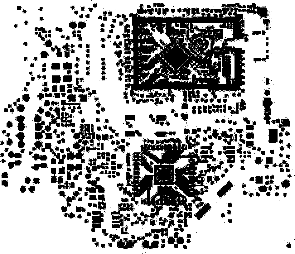
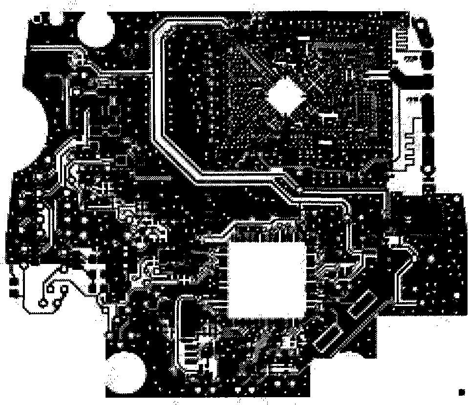
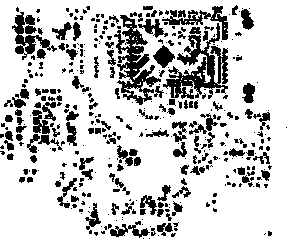
Image

Examples
Embodiment Construction
[0017] The following examples are further explanations and illustrations of the present invention, and do not constitute any limitation to the present invention.
[0018] The steps of the manufacturing method (taking the double-sided panel as an example) of electric nickel and gold circuit boards that can save nickel and gold consumption of the present invention are as follows:
[0019] First, drill holes on the cut and baked copper clad board according to the program compiled by the customer, and then perform copper sinking and copper plating on the drilled holes to make the circuits on both sides of the copper clad board conductive. The above steps are the same as the conventional process.
[0020] The gist of the present invention is that, by forming the secondary circuit on the circuit board, the circuit pattern is selectively electro-nickel and electro-gold, and the specific steps are:
[0021] a. Paste a layer of dry film on the copper-plated circuit board. The dry film ...
PUM
 Abstract
Description
Claims
Application Information