Making method of electric nickel and golden circuit board for saving nickel and gold dosage

A production method and circuit board technology, applied in the manufacture of printed circuits, removal of conductive materials by chemical/electrolytic methods, printed circuits, etc., to save precious metals nickel and gold, and reduce production costs

Inactive Publication Date: 2011-04-06
陈国富
View PDF4 Cites 0 Cited by
  • Summary
  • Abstract
  • Description
  • Claims
  • Application Information

AI Technical Summary

Problems solved by technology

Because in the traditional electro-nickel and electro-gold process, nickel and gold need to be plated on all conductive patterns, so a large amount of nickel and gold need to be consumed, and nickel and gold are precious metals. Partial nickel and gold plating not only reflects the major defects of the traditional process, but also directly leads to the waste of precious metals, and greatly increases the production cost of the enterprise

Method used


Image

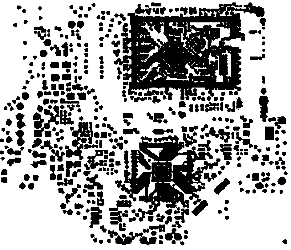
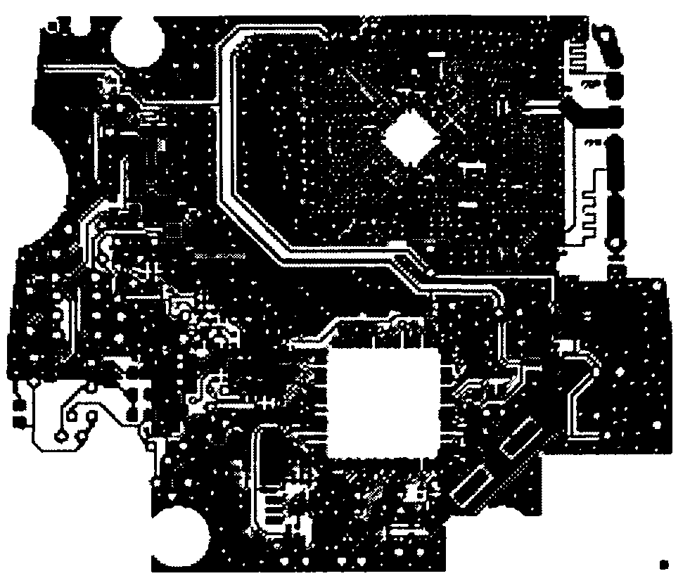
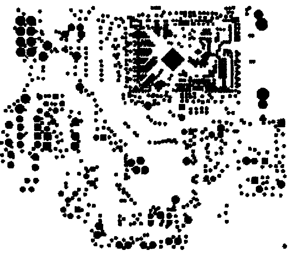
  • Making method of electric nickel and golden circuit board for saving nickel and gold dosage
  • Making method of electric nickel and golden circuit board for saving nickel and gold dosage
  • Making method of electric nickel and golden circuit board for saving nickel and gold dosage

Examples


Embodiment Construction

[0019] The following examples are further explanations and illustrations of the present invention, and do not constitute any limitation to the present invention.

[0020] The steps of the method for making an electro-nickel and gold circuit board that can save nickel and gold consumption (taking a double-sided board as an example) of the present invention are as follows:

[0021] First, drill holes on the cut and baked CCL according to the program prepared by the customer, and then perform copper immersion and copper plating on the drilled holes to make the circuits on both sides of the CCL conduct. The above steps are the same as the conventional process.

[0022] The gist of the present invention is that by forming a secondary circuit on the circuit board, the circuit pattern can be selectively electro-nickel and electro-gold. The specific steps are:

[0023] a. A layer of dry film is pasted on the copper-plated circuit board, and the dry film is a water-soluble dry film, wh...


PUM


Abstract

A manufacturing method of an electrolytic nickel and gold wiring board capable of saving dosage of nickel and gold, comprises broaching, copper precipitation, and copperizing on a copper-coated plate. The method is characterized by further comprising: a, adhering a dry film or printing a wet film on the wiring board, then adhering a positive sheet, exposing and developing to form a primary circuit; b, electroplating nickel and gold on all positions to be welded and copper surfaces of metal holes, then stripping; c, printing a wet film or adhering a dry film, then adhering a negative sheet, exposing and developing to form a secondary circuit; d, etching a circuit diagram, removing non-circuit portions, holding circuit portions, then performing stripping and etching detection; e, performingdeoxidation treatment to the wiring board to remove oxides on the copper surfaces; f, after deoxidation treatment, resistance welding, exposing, developing, printing element symbols and machining shapes so as to manufacture the electrolytic nickel and gold wiring board only at the positions to be welded and the metal hole positions. With the method, the area of the nickel and gold can be reduced by 40-60%, thereby saving the noble metal nickel and gold and effectively reducing enterprise production cost.

Description

【Technical field】 [0001] The invention relates to a printed circuit board (PCB), in particular to a method for manufacturing an electro-nickel and gold circuit board which can reduce the plated area by up to 90% compared with a traditional circuit board and can save nickel and gold consumption. 【Background technique】 [0002] As we all know, printed circuit boards (PCBs) are used in almost all electronic devices we can see, ranging from electronic watches, calculators, general-purpose computers, to computers, electronic communication equipment, military weapon systems, etc., as long as There are electronic components such as integrated circuits, and PCBs are used for electrical interconnection between them. Printed circuit boards are formed by setting conductive patterns for electrical connections between electronic components on an insulating substrate, and its manufacturing process is relatively complicated. On printed circuit boards with higher requirements, nickel and ...

Claims


Application Information

Patent Timeline
Patent Type & Authority Patents(China)
IPC IPC(8): H05K3/00H05K3/06
CPCH05K3/243H05K2203/0723H05K3/064
Inventor 陈国富
Owner 陈国富
Why Eureka
Try Eureka