LED encapsulation structure and forming method thereof

A technology of LED packaging and molding method, applied in electrical components, electrical solid devices, circuits, etc., can solve the problems of single refractive index of packaging materials, poor heat dissipation of epoxy resin, low external quantum efficiency, etc., to avoid single refractive index, The effect of improving heat dissipation performance and high external quantum efficiency

Inactive Publication Date: 2008-09-24
深圳市量子光电子有限公司
View PDF0 Cites 12 Cited by
  • Summary
  • Abstract
  • Description
  • Claims
  • Application Information

AI Technical Summary

Problems solved by technology

Usually, the LED package body 42 is packaged with epoxy resin. Due to the poor heat dissipation of epoxy resin, when the LED is lit, the LED chip 41 will generate a lot of heat, and the epoxy resin cannot dissipate the heat in time, resulting in LED Chip 41 continues to operate at high temperature, resulting in a large light attenuation
[0005] In addition, when the light emitted by the LED luminous material passes through the chip 41 and enters the epoxy resin package, it will be refracted. The refractive index of th

Method used


Image

  • LED encapsulation structure and forming method thereof
  • LED encapsulation structure and forming method thereof
  • LED encapsulation structure and forming method thereof

Examples


Embodiment Construction

[0019] In order to make the object, technical solution and advantages of the present invention clearer, the present invention will be further described in detail below in conjunction with the accompanying drawings and embodiments. It should be understood that the specific embodiments described here are only used to explain the present invention, not to limit the present invention.

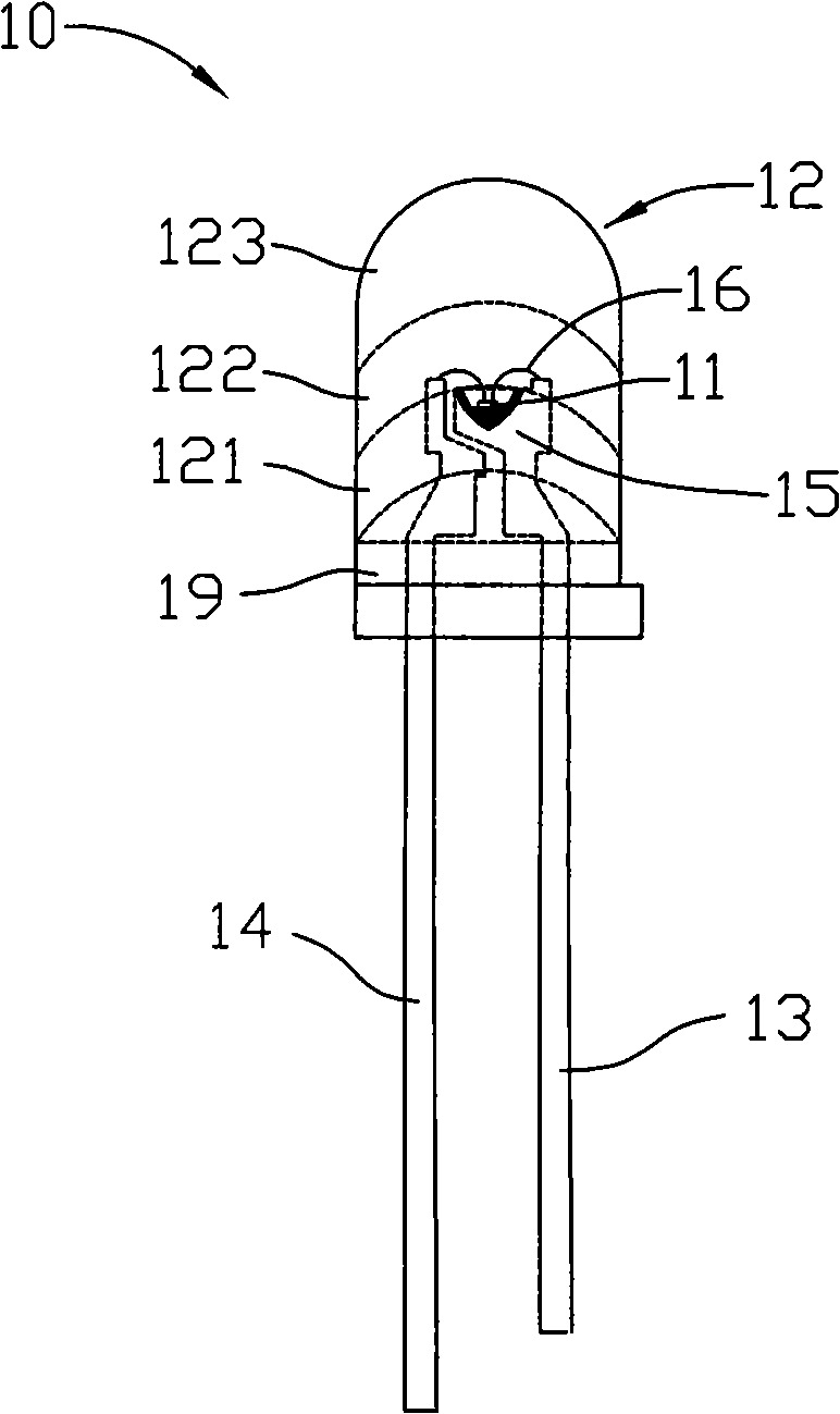
[0020] see figure 2 , is the LED packaging structure 10 provided by the first embodiment of the present invention. The LED packaging structure 10 includes an LED chip 11, an LED package body 12, two brackets 13 and 14 protruding from the package body 12, a cup body 15 for accommodating the LED chip 11, and two brackets connecting the LED chip 11 and the brackets 13 and 14. Metal wire 16.

[0021] The LED chip 10 can be a solid semiconductor chip, and its luminescent material can be blue GaN or GaInN material, and of course other luminescent materials that can emit red, orange, yellow, green, blu...


PUM


Abstract

The invention relates to an LED encapsulation structure, which comprises an LED chip, a cup body for housing the LED chip, an LED encapsulation body and a supporter which extends out of the encapsulation body and is electrically connected with the LED chip. The encapsulation body comprises a multi-layer silica gel, the index of refraction of which is reduced layer by layer from the inside out accordingly to the LED chip. The invention also relates to a molding method of the LED encapsulation structure. The LED encapsulation structure adopts the multi-layer silica gel with the index of refraction reduced layer by layer, which not only provides better heat dissipation, but also avoids the single index of refraction of the encapsulation material, thus increasing the angle of total reflection of an LED lens, improving the utility rate of luminous energy and acquiring the extremely high external quantum efficiency.

Description

technical field [0001] The invention relates to light-emitting components, in particular to an in-line LED packaging structure and a forming method thereof. Background technique [0002] LED (Light Emitting Diode), that is, light emitting diode, is a semiconductor solid light emitting device. It uses solid semiconductor chips as light-emitting materials. When a forward voltage is applied to both ends, the minority interceptors and the majority interceptors in the semiconductor recombine, releasing excess energy and causing photon emission, directly emitting red, orange, yellow, green, blue, blue, purple light. LED light sources are widely used due to their advantages of high energy saving, long life, and environmental protection. [0003] LEDs generally include the following categories: in-line LEDs (DIP LEDs), patch LEDs (SMD LEDs), glue-filled patch LEDs (TOP LEDs), and high-power LEDs (POWER LEDs). Among them, the in-line LED has the advantages of high brightness, high...

Claims


Application Information

Patent Timeline
IPC IPC(8): H01L33/00H01L33/52
CPCH01L2224/48091H01L2224/48247
Inventor 刘镇李军
Owner 深圳市量子光电子有限公司
Why Eureka
Try Eureka