
Plasma treatment apparatus and short circuit of high frequency current

A processing device and plasma technology, applied in the direction of plasma, circuit, discharge tube, etc., can solve the problems of insufficient space, difficulty in increasing the number of short circuit boards 58, failure to eliminate the potential difference of the grounding substrate, etc.

Inactive Publication Date: 2008-10-22
TOKYO ELECTRON LTD
View PDF0 Cites 12 Cited by
  • Summary
  • Abstract
  • Description
  • Claims
  • Application Information

AI Technical Summary

Problems solved by technology

[0007] In order to lower the potential of the ground substrate 55, it is most effective to increase the number of short-circuit plates 58. However, since structural components such as lift pins (not shown) are arranged in the lower space, there is not enough space and it is difficult to increase the number of short-circuit plates. The number of short circuit boards 58
[0008] Therefore, the potential difference between the ground substrate 55 and the wall surface of the chamber 51 is still not eliminated, and there is a possibility that capacitively coupled plasma and abnormal discharge may be generated in the lower space due to the potential difference.

Method used


Image

  • Plasma treatment apparatus and short circuit of high frequency current
  • Plasma treatment apparatus and short circuit of high frequency current
  • Plasma treatment apparatus and short circuit of high frequency current

Examples


Embodiment Construction

[0047] Hereinafter, embodiments of the present invention will be described with reference to the drawings.

[0048] First, a plasma processing apparatus according to a first embodiment of the present invention will be described.

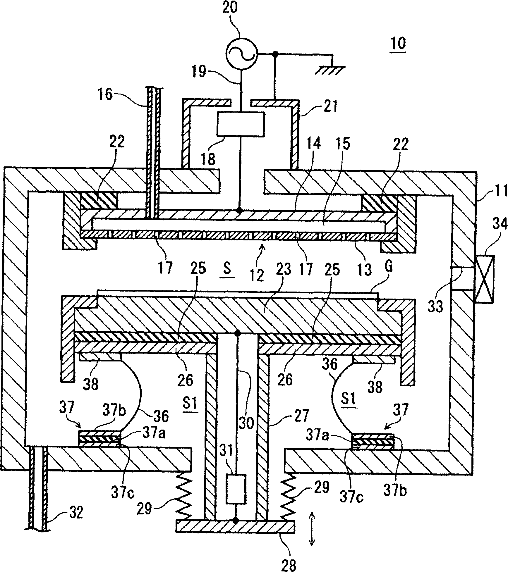
[0049] figure 1 It is a cross-sectional view schematically showing the structure of the plasma processing apparatus of this embodiment. This plasma processing apparatus is configured to perform an etching process on a glass substrate for a liquid crystal display (LCD).

[0050] exist figure 1 Among them, the plasma processing apparatus 10 has, for example, a rectangular cylinder-shaped chamber 11 (storage container) for accommodating a rectangular glass substrate (hereinafter referred to as "substrate") G having a side of approximately 1 m. The chamber 11 is made of aluminum, and most of the inner walls of the chamber 11 are covered with alumite.

[0051] On the top of the chamber 11, a shower head 12 (upper electrode) is arranged. The shower h...


PUM


Abstract

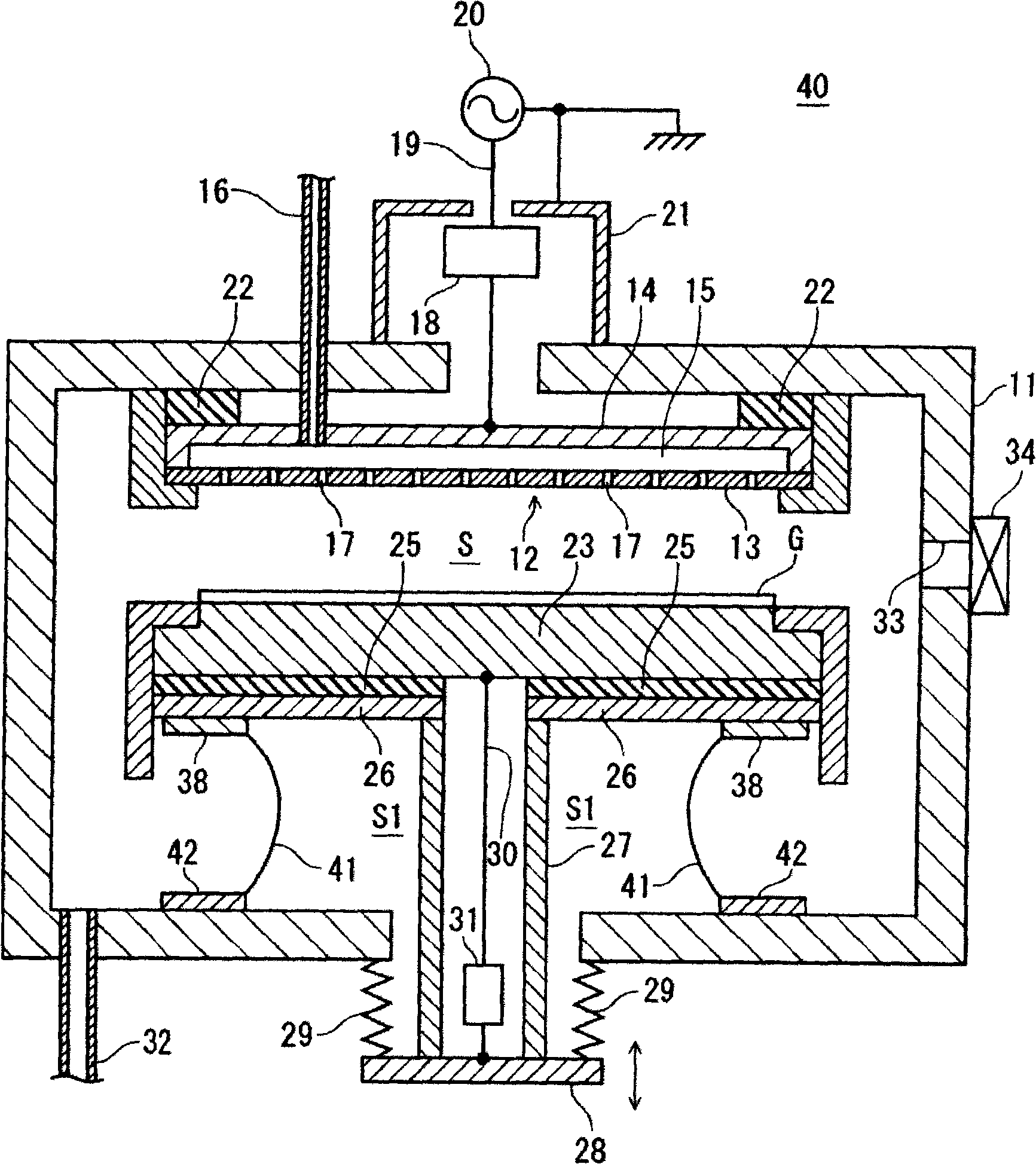
The invention provides a plasma treatment apparatus capable of reducing potential difference between a ground substrate which holds at least either a lower electrode or an upper electrode, and the inner wall of a housing vessel. The plasma treatment apparatus 10 includes: a chamber 11 for housing a glass substrate G; a lower electrode board 23 as a mounting face, which is arranged in the chamber 11 for mounting the glass substrate G; a shower head 12 arranged facing the lower electrode board 23 for supplying raw gas into the chamber 11; a high-frequency power supply 20 connected to the upper electrode 13 of the shower head 12; a ground substrate 26 placed in a state of being spaced apart from the inner wall of the chamber 11, while supporting the lower electrode board 23 through a lower insulation part 25; and a shorting bar 36 for shunting the ground substrate 26 and the inner wall of the chamber 11. A capacitor 37 is interposed between the shorting bar 36 and the inner wall of the camber 11, and is provided on the inner wall of the camber 11.

Description

technical field [0001] The present invention relates to a plasma processing device and a short-circuit circuit for high-frequency current, in particular to a plasma processing device for performing plasma processing on a substrate. Background technique [0002] Such as Image 6 As shown, a plasma processing apparatus 50 for performing etching treatment on glass substrates for seventh-generation and eighth-generation liquid crystal panels includes: a chamber 51 for accommodating a glass substrate (hereinafter referred to as "substrate") G; the lower electrode 52 of G; and the upper electrode 54 of the shower head 53 facing the lower electrode 52 . In this plasma processing apparatus 50, the processing gas supplied to the space between the upper electrode 54 and the lower electrode 52 (hereinafter referred to as "processing space") is excited by a high-frequency electric field to generate plasma. The substrate G is etched. [0003] In the plasma processing apparatus 50 , the...

Claims


Application Information

Patent Timeline
Patent Type & Authority Applications(China)
IPC IPC(8): H01L21/00H01L21/3065H01J37/32H05H1/46
CPCH01J37/32174H01J37/32477H01J37/32532H05H1/46H05H1/4652H05H2242/20
Inventor 佐佐木和男中村充一
Owner TOKYO ELECTRON LTD
Learn More