Method for manufacturing bonded substrate
A technology for laminating substrates and manufacturing methods, applied in semiconductor/solid-state device manufacturing, electrical components, circuits, etc., can solve problems such as operational errors, difficulty in taking out, difficulty in identifying the surface and the back, and achieve the effect of preventing direct contact
- Summary
- Abstract
- Description
- Claims
- Application Information
AI Technical Summary
Problems solved by technology
Method used
Image

Examples
Embodiment 1
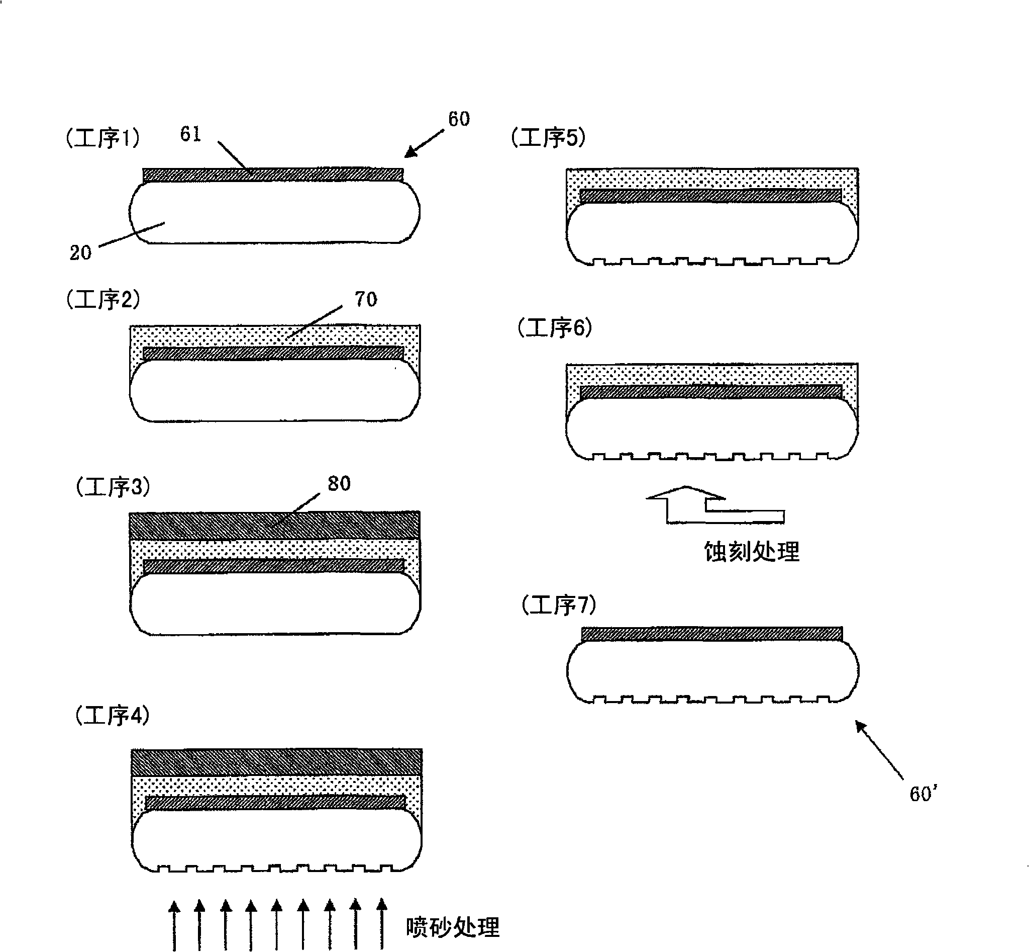
[0114] A bonded substrate was produced by implementing the method for producing a bonded substrate of the present invention to roughen the back surface.
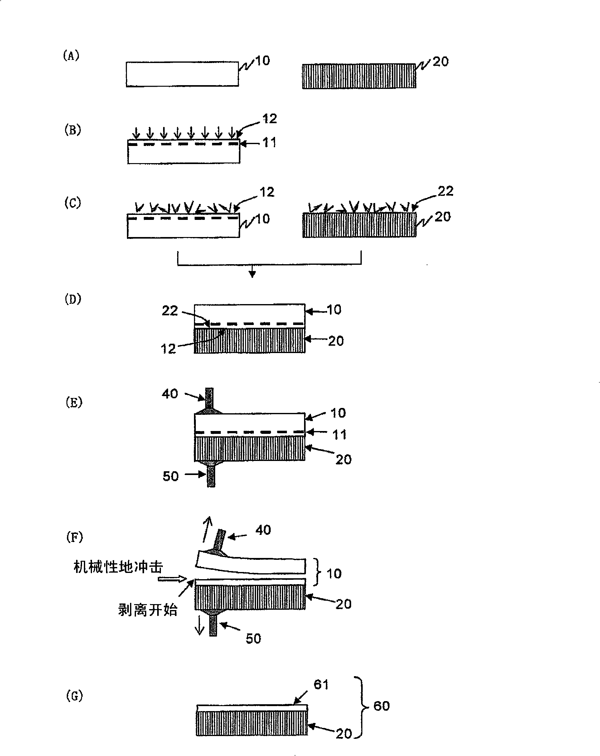
[0115] A silicon substrate with a diameter of 150 mm was prepared as a donor wafer, and a silicon oxide film of 100 nm was formed on the surface thereof by thermal oxidation. Hydrogen ions are implanted into the substrate through the silicon oxide film to form an ion implantation layer. The ion implantation conditions are implantation energy of 35keV, implantation dose of 9×10 16 / cm 2 , The implantation depth is 0.3nm.
[0116] Furthermore, a quartz substrate with a diameter of 150 mm was prepared as a support sheet.
[0117] Next, using a plasma processing apparatus, nitrogen gas was introduced as a gas for plasma, and surface activation treatment was performed on the ion-implanted surface of the prepared silicon substrate and the surface of the quartz substrate.
[0118] Then, a bonded substrate was produced. These su...
Embodiment 2
[0125] The same sample wafer as in Example 1 was prepared.
[0126] A dicing tape was directly attached as a protective tape to the surface of the silicon thin film side of the sample wafer, and the back surface of the sample wafer was subjected to sandblasting in the same manner as in Example 1.
[0127]After blasting, the dicing tape is peeled off from the silicon film and cleaned with ultrasonic water. Then, by immersing the sample wafer in a hydrofluoric acid solution, the back surface of the sandblasting sample wafer (the back surface of the quartz substrate) was etched to manufacture a bonded substrate with a roughened back surface.
[0128] In this way, for the bonded substrate produced by the production method of the present invention, when evaluating the state of the front surface and the back surface, although some peeling of the silicon thin film from the quartz substrate and peeling of the surface of the silicon thin film were confirmed on the front side, it was st...
PUM
 Abstract
Description
Claims
Application Information
 - R&D
- Intellectual Property
- Life Sciences
- Materials
- Tech Scout
- Unparalleled Data Quality
- Higher Quality Content
- 60% Fewer Hallucinations
Browse by: Latest US Patents, China's latest patents, Technical Efficacy Thesaurus, Application Domain, Technology Topic, Popular Technical Reports.
© 2025 PatSnap. All rights reserved.Legal|Privacy policy|Modern Slavery Act Transparency Statement|Sitemap|About US| Contact US: help@patsnap.com