Resistive memory device and stack structure of resistive random access memory device

A resistive memory, resistive random technology, applied in static memory, digital memory information, magnetic field controlled resistors, etc., can solve problems such as difficult sensing, and achieve the effect of improving resistivity and increasing coherence

Active Publication Date: 2010-07-21
TAIWAN SEMICON MFG CO LTD
View PDF0 Cites 0 Cited by
  • Summary
  • Abstract
  • Description
  • Claims
  • Application Information

AI Technical Summary

Problems solved by technology

However, the typical structure in which the above-mentioned dielectric material is sandwiched between two electrode layers like a sandwich structure often leads to a lower resistivity (resistance ratio, Ron / Roff) of a conventional RRAM cell. ) are relatively low and are often difficult to sense in some applications

Method used


Image

  • Resistive memory device and stack structure of resistive random access memory device
  • Resistive memory device and stack structure of resistive random access memory device
  • Resistive memory device and stack structure of resistive random access memory device

Examples


Embodiment Construction

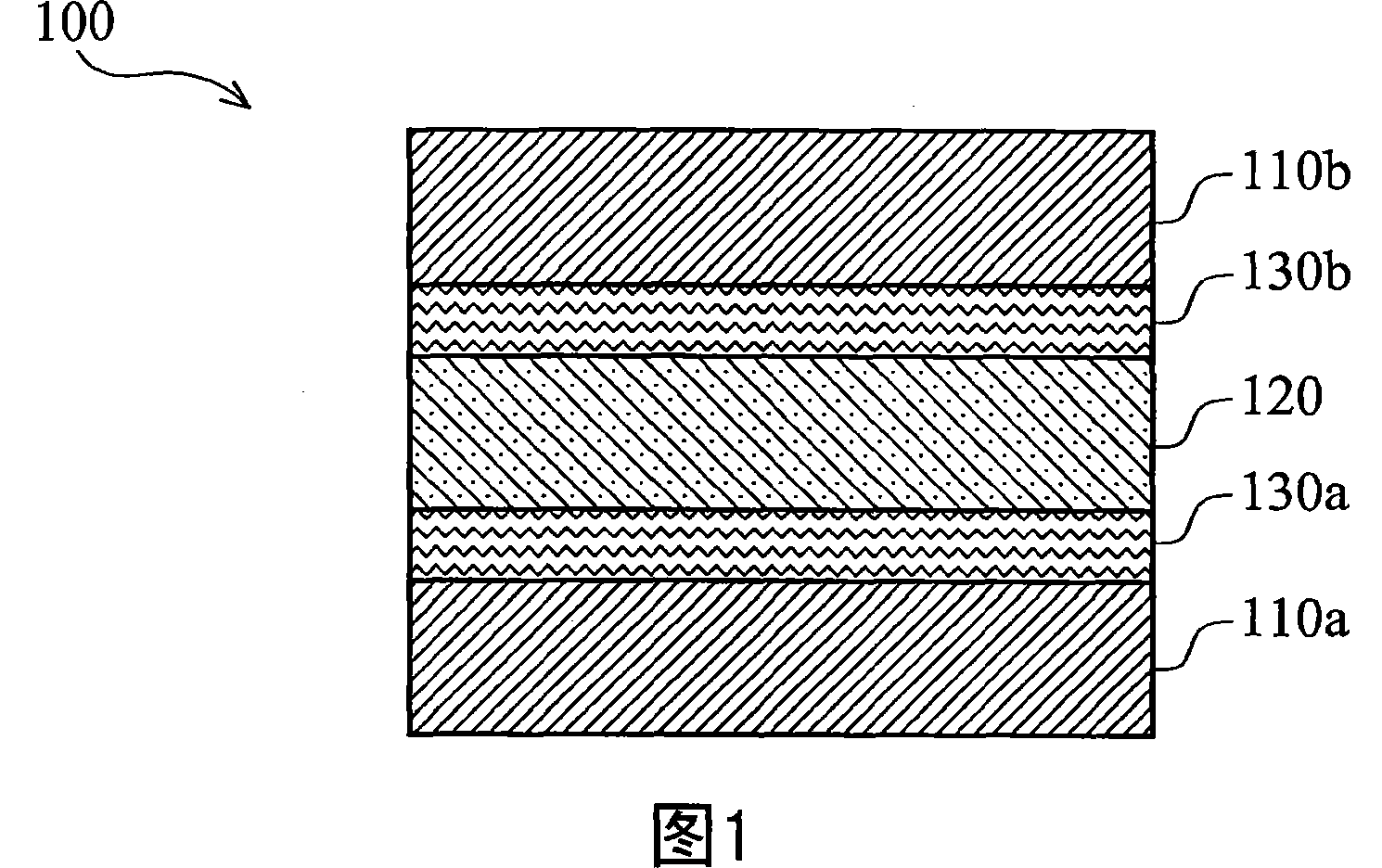
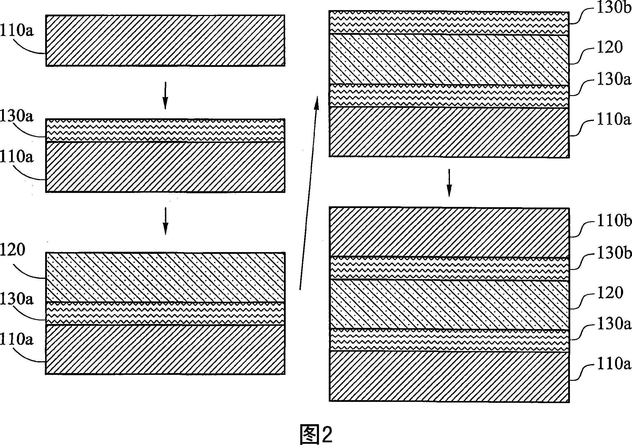
[0040] Please refer to the embodiment shown in FIG. 1, which shows the RRAM stacked layer 100 used in a resistive random access memory (RRAM) monolithic structure, and its method of processing according to the principles disclosed herein. As previously understood, the RRAM stack 100 includes bottom and top electrode layers 110a, 110b. In an exemplary embodiment, the bottom and top electrode layers 110a, 110b may be composed of conductive materials. For example, the bottom and top electrode layers 110a, 110b can be composed of platinum (Pt) or any useful conductive material.

[0041] The RRAM stack 100 also includes an intermediate dielectric layer 120 between the bottom and top electrode layers 110a, 110b. In the representative embodiment, the intermediate dielectric layer 120 is composed of a Colossal Magnetoresistive (CMR) material. In a specific embodiment, the dielectric layer 120 is made of a dielectric material Pr 1-x Ca x MnO 3 (PCMO). Of course, any dielectric material...


PUM


Abstract

Disclosed herein are new resistive memory devices having one or more buffers layer surrounding a dielectric layer. By inserting one or more buffer layers around the dielectric layer of the device, the resistive ratio of the device is highly enhanced. For example, tests using this unique stack structure have revealed a resistance ratio of approximately 1000x over conventional electrode-dielectric-electrode stack structures found in resistive memory devices. This improvement in the resistance ratio of the resistive memory device is believed to be from the improved interface coherence, and thus smoother topography, between the buffer layer(s) and the dielectric layer.

Description

technical field [0001] The present invention relates to semiconductor integrated circuit devices, and more particularly to resistive memory devices having a buffer layer to increase the resistivity of the memory device. Background technique [0002] As the development of the traditional memory cell (memory cell) structure has approached the size limit, there have been a large number of academic researches to develop many types of memory cell structures, for example, variable resistive (variable resistive element type) memory cells, such as magnetoresistive Magnetic random access memory (MRAM), resistive random access memory (RRAM), and similar devices have continued to gain attention. In the variable resistance memory cell, the difference of the storage state will appear along with the difference of the threshold voltage of the memory transistor (memory transistor). Among resistive memories, RRAM is a good choice for small size applications due to its low operating voltage,...

Claims


Application Information

Patent Timeline
Patent Type & Authority Patents(China)
IPC IPC(8): H01L43/08H01L45/00H01L27/22H01L27/24G11C11/15G11C11/56G11C13/00
CPCG11C11/5685G11C2213/31G11C13/0007G11C11/5678G11C13/0004G11C11/16G11C2213/55
Inventor 邓端理吴泰伯张文渊李自强
Owner TAIWAN SEMICON MFG CO LTD
Why Eureka
Try Eureka