Method for forming fine pattern of semiconductor device

A fine pattern and semiconductor technology, which is applied in the direction of semiconductor devices, semiconductor/solid-state device manufacturing, electrical components, etc., can solve the problems of unobtainable pattern, inaccurate alignment and poor pattern overlapping, so as to avoid misalignment and improve efficiency , The effect of simplifying the process steps

Inactive Publication Date: 2008-11-05
SK HYNIX INC
View PDF1 Cites 13 Cited by
  • Summary
  • Abstract
  • Description
  • Claims
  • Application Information

AI Technical Summary

Problems solved by technology

Therefore, the double patterning technique cannot obtain the desired pattern
Misregistration can occur due to inaccurate pattern overlay during the alignment process

Method used


Image

  • Method for forming fine pattern of semiconductor device
  • Method for forming fine pattern of semiconductor device
  • Method for forming fine pattern of semiconductor device

Examples


Embodiment Construction

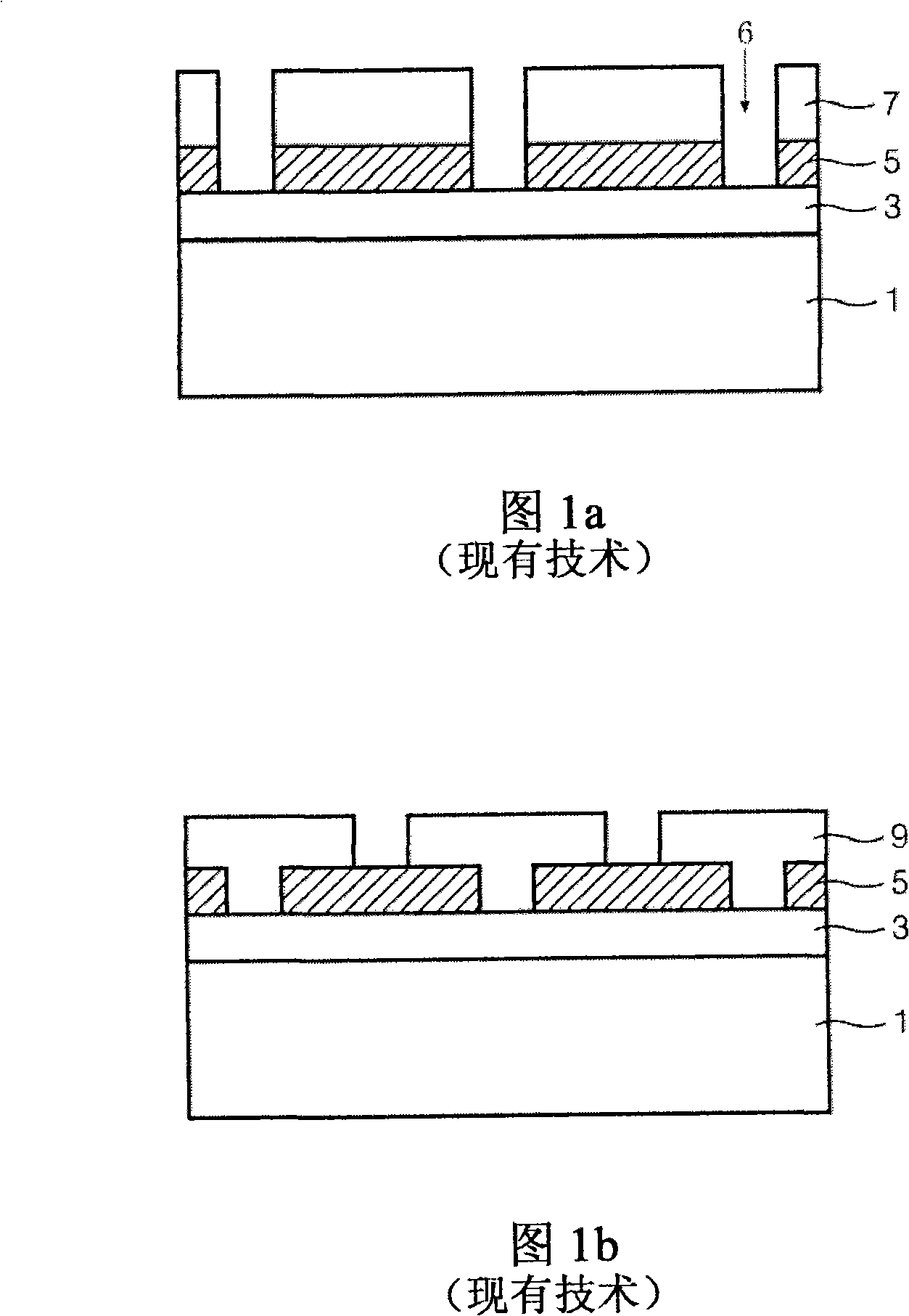
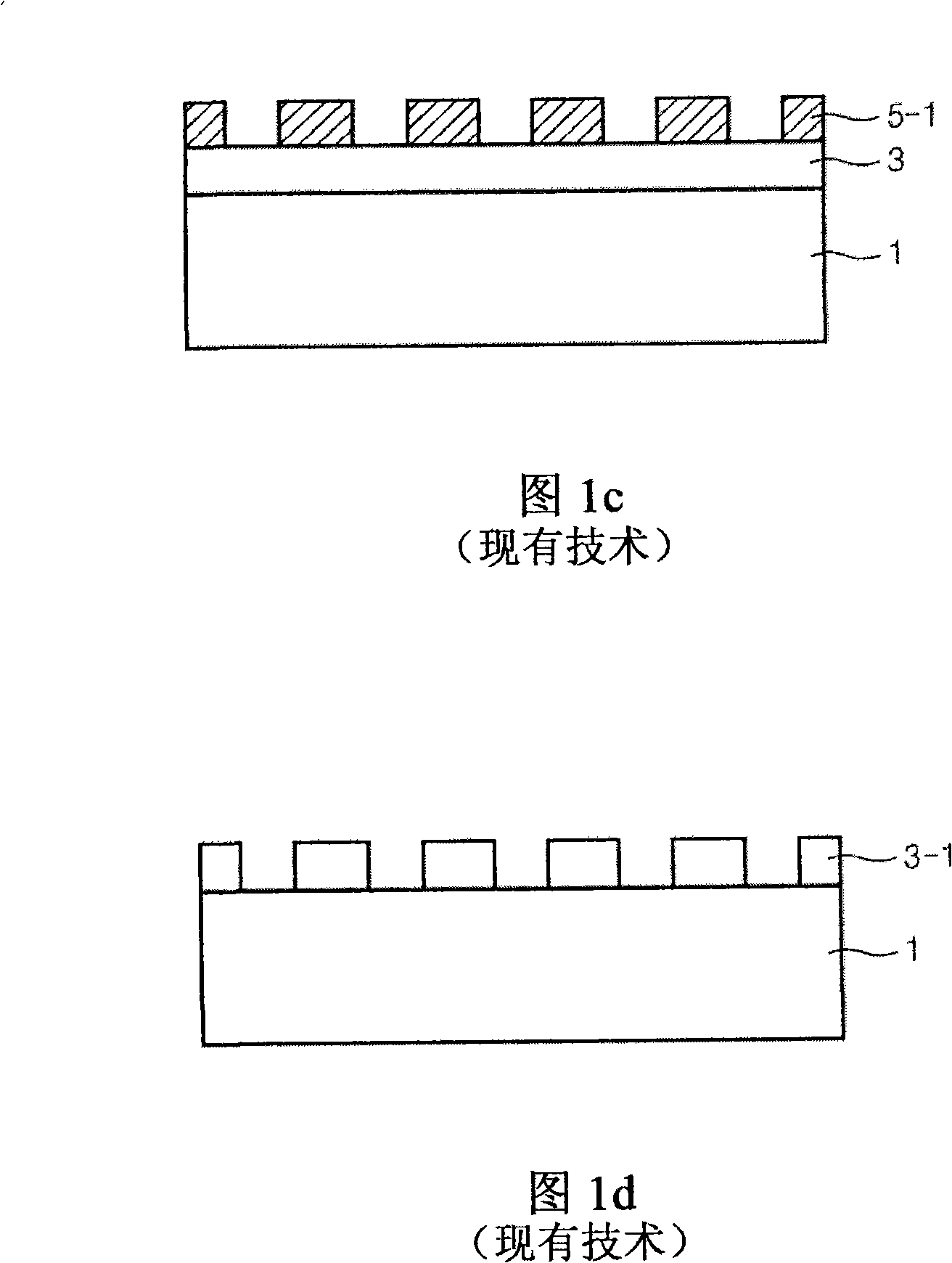
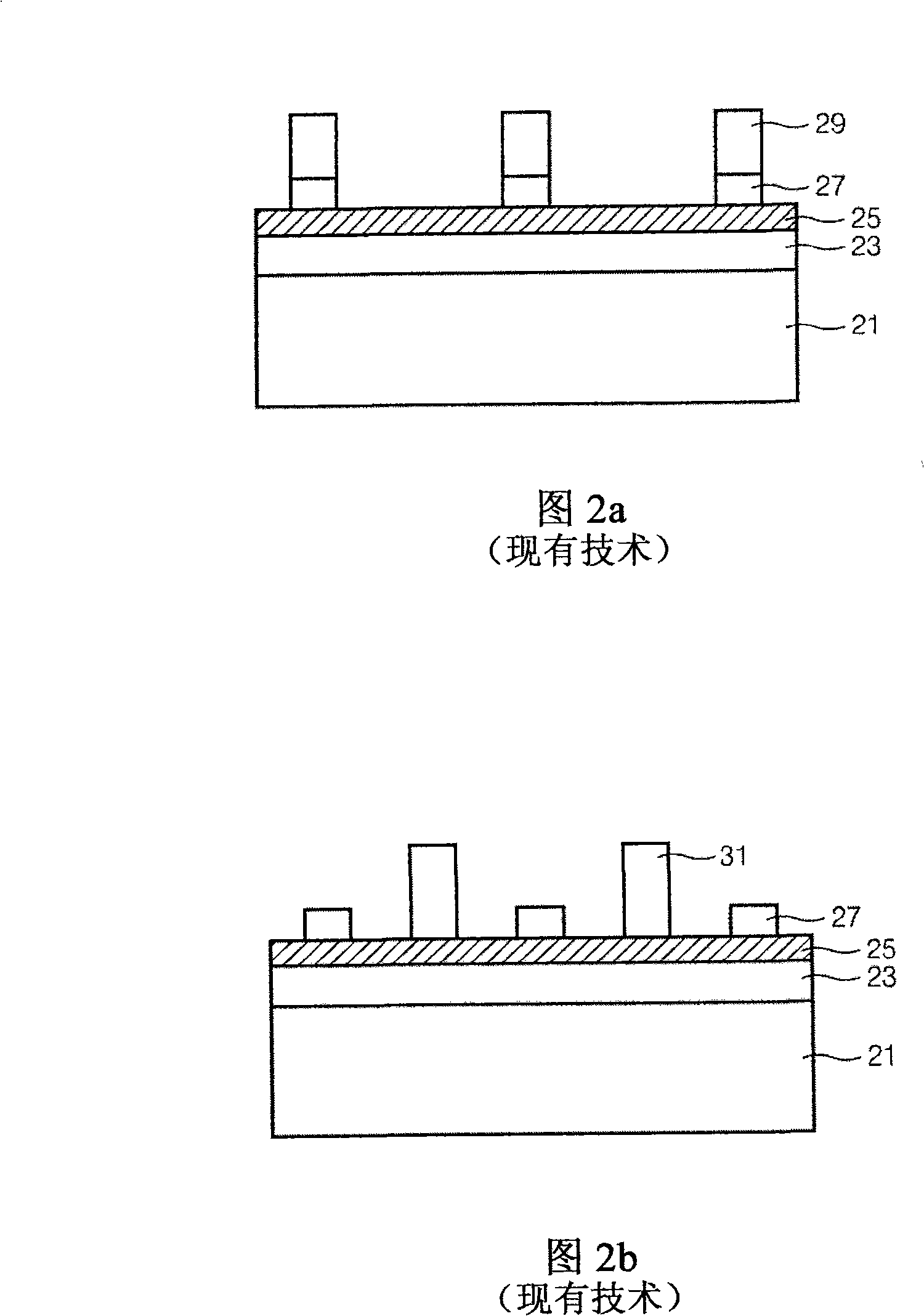
[0018] The double patterning technique for forming fine patterns includes forming grooves to obtain patterns, or forming lines to obtain patterns.

[0019] 1a to 1d are cross-sectional views illustrating a conventional method of forming fine patterns, which includes forming grooves to obtain fine patterns. 2a to 2d are cross-sectional views illustrating a conventional method of forming a fine pattern, which includes forming lines to obtain a fine pattern.

[0020] Referring to FIG. 1 a , a bottom layer 3 , a mask film (not shown) and a first photoresist film (not shown) are deposited on a substrate 1 . A first photolithography process is performed on the first photoresist film to form a first photoresist pattern 7 . Using the first photoresist pattern 7 as an etching mask, a first patterning process is performed on the mask film to form a stack structure including the first mask pattern 5 and the first photoresist pattern 7 and having the trench 6 .

[0021] Referring to FIG...


PUM


Abstract

A method for forming a fine pattern of a semiconductor device includes forming a deposition film over a substrate having an underlying layer. The deposition film includes first, second, and third mask films. The method also includes forming a photoresist pattern over the third mask film, patterning the third mask film to form a deposition pattern, and forming an amorphous carbon pattern at sidewalls of the deposition pattern. The method further includes filling a spin-on-carbon layer over the deposition pattern and the amorphous carbon pattern, polishing the spin-on-carbon layer, the amorphous carbon pattern, and the photoresist pattern to expose the third mask pattern, and performing an etching process to expose the first mask film with the amorphous carbon pattern as an etching mask. The etching process removes the third mask pattern and the exposed second mask pattern.; The method also includes removing the spin-on-carbon layer and the amorphous carbon pattern, and forming a first mask pattern with the second mask pattern as an etching mask.

Description

technical field [0001] The present invention generally relates to methods of forming fine patterns of semiconductor devices. Background technique [0002] With the popularization of information media such as computers, semiconductor device technology has been rapidly developed. Semiconductor devices are required to operate at high speed and to have high memory capacity. As a result, there is a need to manufacture high-capacity semiconductor memory elements with higher integration, reliability, and data access characteristics. [0003] In order to increase the integration of devices, photolithography has been developed to form fine patterns. Photolithography techniques include exposure techniques using chemically amplified deep ultraviolet (DUV) light sources such as ArF (193nm) and VUV (157nm), and techniques of developing photoresists suitable for exposure light sources. [0004] As semiconductor devices become smaller, it is important to control the critical dimension o...

Claims


Application Information

Patent Timeline
Patent Type & Authority Applications(China)
IPC IPC(8): H01L21/033H01L21/311
CPCH01L21/0337H01L21/0338Y10S438/952
Inventor 卜喆圭潘槿道
Owner SK HYNIX INC
Why Eureka
Try Eureka