Detection and package equipment of IC chip

A technology of integrated circuits and packaging equipment, which is applied in the field of testing and packaging equipment, can solve the problems of not being able to meet the actual needs of production flow operations, not being able to meet multiple types/specifications of chips at the same time, and low production efficiency, so as to achieve a fast and efficient testing process. Avoid backlog/disjoint, reduce labor intensity effect

Inactive Publication Date: 2008-12-03
上海允科自动化有限公司
View PDF0 Cites 3 Cited by
  • Summary
  • Abstract
  • Description
  • Claims
  • Application Information

AI Technical Summary

Problems solved by technology

[0005] At present, most of the machines used for the detection and packaging of integrated circuit chips can only complete one process of detection or packaging, and the production efficiency is low.

Method used


Image

  • Detection and package equipment of IC chip

Examples


Embodiment Construction

[0017] The present invention will be further described below in conjunction with the accompanying drawings and embodiments.

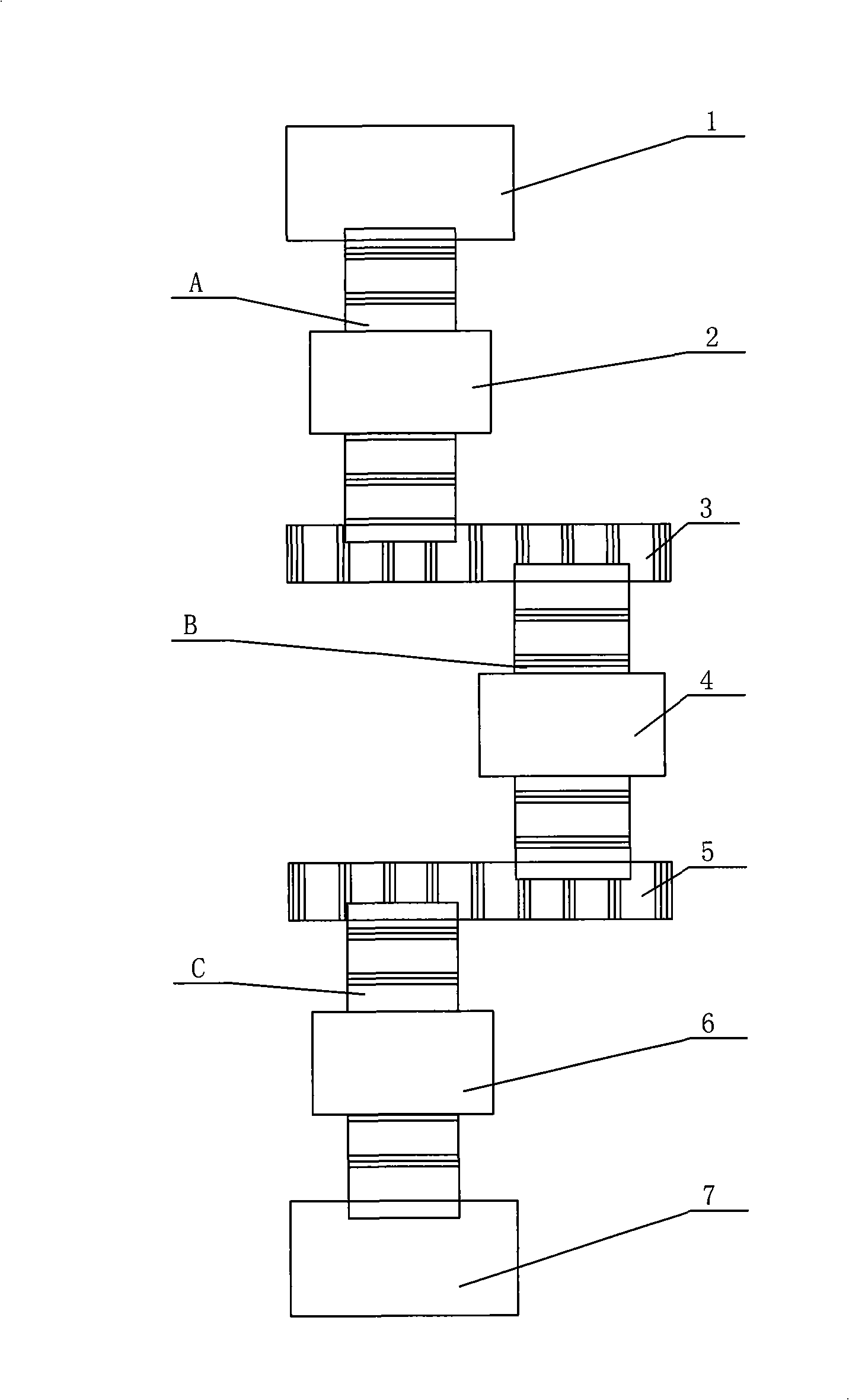
[0018] In Fig. 1, the present invention includes a loading unit, a mark detection unit, a pin detection unit, an exchange area unit, an unqualified area unit, a pick-and-place unit for chips, and a braiding and rolling unit, which is provided with a device to ensure the connection of the above-mentioned units. The main track and the conveyor belt run through the above-mentioned units into a complete process device.

[0019] The main track is composed of three different conveyor belts, which are called No. 1 conveyor belt, No. 2 conveyor belt, and No. 3 conveyor belt; the No. 1 conveyor belt and No. 3 conveyor belt are in a straight line, and the No. Two parallel; three conveyor belts are provided with a supporting plate, used to support the transported pallets, respectively driven by their respective stepping motors and synchronous pulleys with double s...


PUM


Abstract

The invention relates to an apparatus for detecting and packing integrated circuit chips, and belongs to the field of a semiconductor device manufacturing apparatus. A main track and a conveying belts are arranged among a loading unit, an identification detecting unit, a pin detecting unit, an exchanging area unit, an unqualified area unit, a chip picking and placing unit and a braiding and coiling unit; a belt penetrates through each unit for forming a complete procedure device; the main track is composed of three conveying belts, wherein a first conveying belt and a third conveying belt are arranged on one line, and a second conveying belt is parallel to the other two belt conveying belts; double sliding blocks of the three conveying belts are respectively driven by stepper motors and synchronous pulleys, and the three conveying belts keep uninterrupted transmitting motion along a guide rail for carrying a tray to a requested position along the main track. By integrating the functions of labeling, pin detection and coil packing, the apparatus has the advantages of rapid detection process, high working efficiency, and reasonable and ordered production process, thereby avoiding the backlog or the dislocation of each production procedure and each production link. The apparatus is widely applicable to the detecting and packing field of various integrated circuit chips.

Description

technical field [0001] The invention belongs to the field of methods or equipment for manufacturing or processing semiconductor or solid devices or parts thereof, and in particular relates to a detection and packaging equipment for integrated circuit chips. Background technique [0002] In the semiconductor industry, the packaged integrated circuit chip needs to be effectively detected and packaged before it is used as a patch component; After the standard image is compared, it is detected whether the position is qualified. At the same time, the lead (Leader) of the integrated circuit needs to be compared with the standard image through the three-dimensional visual imaging technology to detect whether the parameters of the lead are qualified. [0003] The sorting process after the inspection is to put the good and bad products into different trays by category. The packaging of the final product is to put the inspected chip from the tray into the tape and roll it. [0004] ...

Claims


Application Information

Patent Timeline
Patent Type & Authority Applications(China)
IPC IPC(8): G01R31/28G01R31/01
Inventor 柯恩清
Owner 上海允科自动化有限公司
Why Eureka
Try Eureka