Semiconductor device

A semiconductor and device technology, applied in the field of semiconductor devices, can solve problems such as crystal defects

Inactive Publication Date: 2008-12-03
NEC ELECTRONICS CORP
View PDF1 Cites 0 Cited by
  • Summary
  • Abstract
  • Description
  • Claims
  • Application Information

AI Technical Summary

Problems solved by technology

[0017] For this reason, during the manufacturing process of the semiconductor device 100, the elongated low-voltage transistor regions 121 to 124 may have crystal defects in their longitudinal directions, and such crystal defects may cause leakage current at the P-N junction.

Method used


Image

  • Semiconductor device
  • Semiconductor device
  • Semiconductor device

Examples


Embodiment Construction

[0027] In the following, reference will be made to figure 1 and figure 2 Embodiments of the present invention are described. However, the same parts as those of the above-mentioned conventional examples will be denoted by the same names, and their detailed descriptions will be omitted.

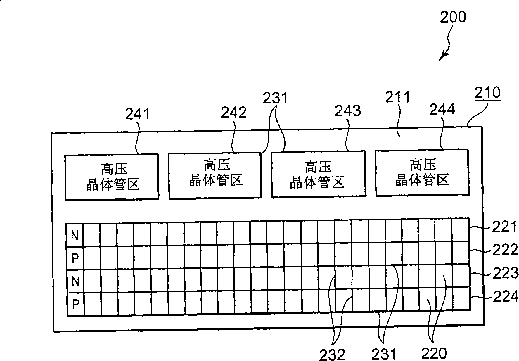
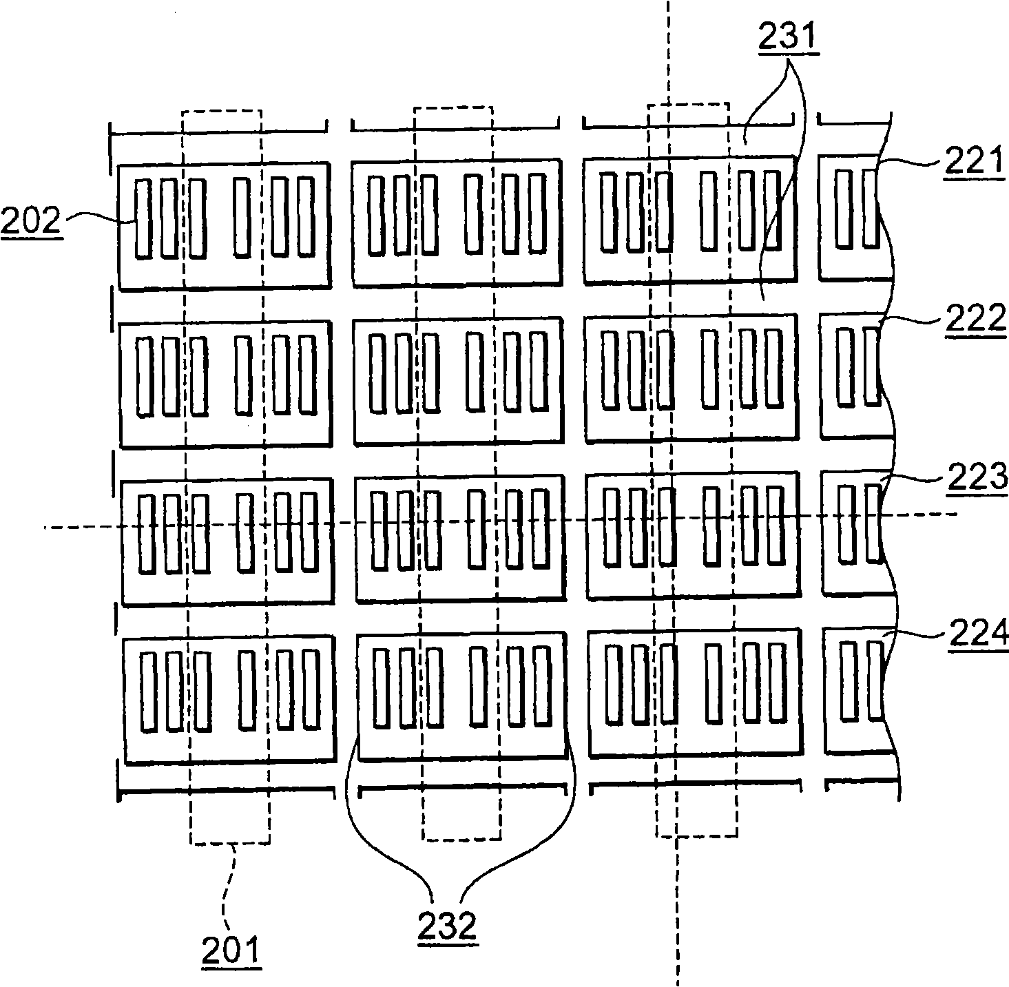
[0028] like figure 1 As shown, the semiconductor device 200 of this embodiment includes: an SOI substrate 210 ; low-voltage transistor regions 221 to 224 ; an element isolation layer 231 ; and a plurality of internal isolation layers 232 . The SOI substrate 210 is a semiconductor substrate on which semiconductor layers 211 are stacked with the semiconductor layers 211 interposed therebetween. The low-voltage transistor regions 221 to 224 are circuit element regions in which a plurality of semiconductor circuits 201 each having the same function are formed in an array in the semiconductor layer 211 . Each element isolation layer 231 is insulating and has a shape that separates the low-vo...


PUM


Abstract

Provided is a semiconductor device that is capable of suppressing occurrence of a crystal defect in an elongated circuit region formed in an SOI substrate. Low-voltage transistor regions are separated, by multiple inner isolation layers, into multiple sub-regions. For this reason, the length of the longitudinal direction of the sub-regions is reduced, even though the low-voltage transistor regions are extremely elongated, for example. This configuration can suppress occurrence of a crystal defect in the low-voltage transistor regions in the longitudinal direction thereof, although such defect may occur due to the difference in thermal expansion or thermal contraction between a semiconductor layer in the low-voltage transistor regions, and the element isolation layers.

Description

technical field [0001] The present invention relates to a semiconductor device in which a semiconductor circuit is formed in an SOI (Semiconductor On Insulator) substrate. More specifically, the present invention relates to a semiconductor device in which a plurality of semiconductor circuits are formed in an array in a circuit element region of an SOI substrate. Background technique [0002] Refer to Figure 4 and Figure 5 , a conventional example of a semiconductor device in which a semiconductor circuit is formed in an SOI substrate will be described hereinafter, Figure 5 is a schematic longitudinal sectional view taken along line X-X' in FIG. 4 . The semiconductor device 100 shown here as an example includes an SOI substrate in which a semiconductor layer 113 is stacked on a semiconductor substrate 111 with an intermediate insulating layer 112 interposed therebetween. [0003] In the semiconductor layer 113, a plurality of low-voltage transistor regions 121 to 124 are ...

Claims


Application Information

Patent Timeline
Patent Type & Authority Applications(China)
IPC IPC(8): H01L27/12H01L21/762
Inventor 伊藤将之藤原章井上胜博
Owner NEC ELECTRONICS CORP
Why Eureka
Try Eureka