Epitaxial wafer for light-emitting diodes
A technology of light-emitting diodes and epitaxial wafers, which is applied in the field of epitaxial wafers for light-emitting diodes, and can solve the problems of shortening the light-emitting wavelength and other issues
- Summary
- Abstract
- Description
- Claims
- Application Information
AI Technical Summary
Problems solved by technology
Method used
Image
Examples
Embodiment 1)
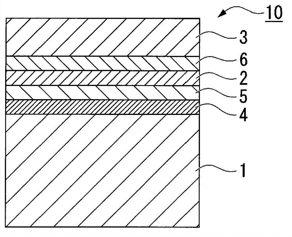
[0145] In the light-emitting diode of Example 1, first, epitaxial growth layers are sequentially stacked on a semiconductor substrate made of Si-doped n-type GaAs single crystal to form an epitaxial wafer. The n-type GaAs substrate uses the plane inclined 15° from the (100) plane to the (0-1-1) direction as the growth plane, and the carrier concentration is set to 2×10 18 cm -3 .
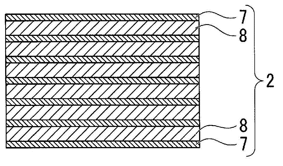
[0146] As the epitaxial growth layer, on the n-type GaAs substrate, a buffer layer composed of Si-doped n-type GaAs, a buffer layer composed of Si-doped n-type (Al 0.5 Ga 0.5 ) 0.5 In 0.5 Low resistance layer composed of P, n-type Al doped with Si 0.5 In 0.5 The lower cladding layer composed of P, undoped Ga as the strained light-emitting layer 0.42 In 0.58 P and undoped (Al 0.53 Ga 0.47 ) 0.51 In 0.49 The light-emitting part where P is alternately stacked, and the p-type Al doped with Mg 0.5 In 0.5 The upper cladding layer composed of P, the (Al 0.6 Ga 0.4 ) 0.5 In 0.5 P, and p-ty...
Embodiment 2)
[0162] In the light-emitting diode of Example 2, instead of the strained light-emitting layer provided in the light-emitting diode of Example 1, an undoped Ga 0.36 In 0.64 Except that P was used as the strained light-emitting layer, it was formed in the same manner as the light-emitting diode of Example 1.
[0163] As shown in Table 1, in the case of the light-emitting diode of Example 1, the following good results were obtained: the peak emission wavelength was 681.5 nm, there were no surface defects, and the deviation of the peak emission wavelength in the substrate plane was as small as 2.6 nm. , the output power was 3.5mW, and the output power ratio before and after the power-on test was 98%.
Embodiment 3)
[0165] In the light-emitting diode of Example 3, instead of the strained light-emitting layer provided in the light-emitting diode of Example 1, an undoped Ga 0.35 In 0.65 P serves as the strained light-emitting layer, and instead of the barrier layer provided in the light-emitting diode of Example 1, an undoped (Al 0.53 Ga 0.47 ) 0.54 In 0.46 P is formed similarly to the light emitting diode of Example 1 except for this.
[0166] As shown in Table 1, in the case of the light-emitting diode of Example 3, the following good results were obtained: the peak emission wavelength was 685.3 nm, there was no surface defect, and the deviation of the peak emission wavelength in the substrate plane was as small as 2.5 nm. , the output power was 3.1mW, and the output power ratio before and after the power-on test was 98%.
PUM
 Abstract
Description
Claims
Application Information


