Manufacturing method for high sensitivity semiconductor nano ultraviolet light detector

A high-sensitivity, semiconductor technology, applied in the electrical field, can solve the problems of poor photocurrent stability, slow response recovery speed, and large dark current, and achieve high-quality crystallization performance, fast response, and low dark current.

Inactive Publication Date: 2017-06-27
UNIV OF SHANGHAI FOR SCI & TECH
View PDF4 Cites 7 Cited by
  • Summary
  • Abstract
  • Description
  • Claims
  • Application Information

AI Technical Summary

Problems solved by technology

[0004] Aiming at the above-mentioned technical problems in the prior art, the invention provides a kind of preparation method of high-sensitivity semiconductor nano-ultraviolet light detector, the preparation method of described this high-sensiti...

Method used


Image

  • Manufacturing method for high sensitivity semiconductor nano ultraviolet light detector
  • Manufacturing method for high sensitivity semiconductor nano ultraviolet light detector
  • Manufacturing method for high sensitivity semiconductor nano ultraviolet light detector

Examples


Embodiment 1

[0034] A method for preparing a two-dimensional ultra-thin structure single crystal ZnO nano-ultraviolet light detector, specifically comprising the following steps:

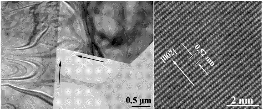
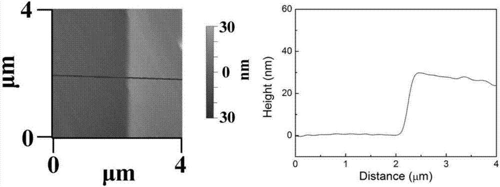
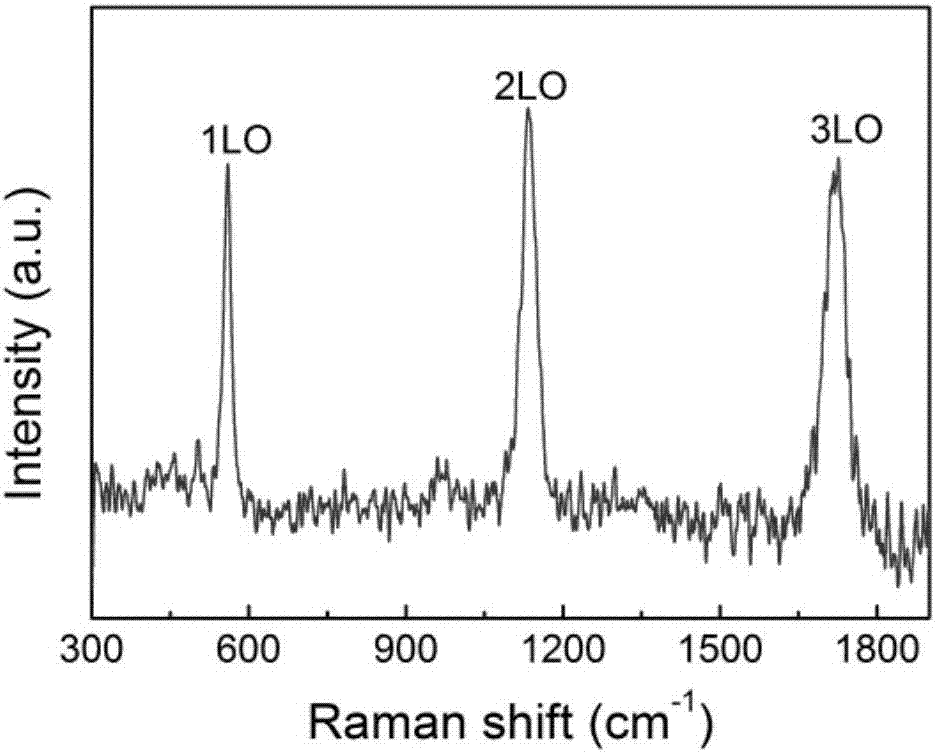
[0035] 1) A step of preparing two-dimensional ultra-thin structure single crystal ZnO nanomaterials by chemical vapor deposition method, and the surface is plated with polished SiO of 0.5~5 nm thick Au, Fe, Ni, Pt, Mo and other metals 2 Or sapphire as the substrate, ZnO or Zn powder with a purity of 99.9%, 100~800 mesh graphite powder with a purity of 99%, phosphorus, antimony, or vanadium oxide powder with a purity of 99% in a mass ratio of 1:0.1~ 5: 0.001~0.05 mixed, fed with oxygen and argon with a purity of 99.99%, and prepared by chemical deposition at 500~1200°C;

[0036] 2) Using methods such as ultrasonic dispersion, spin-coating organic films such as PMMA, PDMS, or PVDF on the two-dimensional ultra-thin structure single-crystal ZnO nanomaterial, or high-purity gas purging, the two-dimensional ultra-thin...


PUM

PropertyMeasurementUnit
Thicknessaaaaaaaaaa
Thicknessaaaaaaaaaa
Thicknessaaaaaaaaaa

Abstract

The invention discloses a manufacturing method for a high sensitivity semiconductor nano ultraviolet light detector. According to the method, firstly, a two-dimensional ultrathin structure monocrystalline ZnO nano material is manufactured; the two-dimensional ultrathin structure monocrystalline ZnO nano material is transfered from a growth substrate; the two-dimensional ultrathin structure monocrystalline ZnO nano material is mixed with organic solution or deionized water; ultrasonic dispersion of the two-dimensional ultrathin structure monocrystalline ZnO nano material solution is carried out; the two-dimensional ultrathin structure monocrystalline ZnO nano material solution is coated on a surface of a semiconductor, insulation and conductive substrate; along a length direction of the two-dimensional ultrathin structure monocrystalline ZnO nano material, and conductive metal electrodes are plated at two ends; a mask is utilized to cover the two-dimensional ultrathin structure monocrystalline ZnO nano material, an insulation oxide covering layer is plated, an insulation oxide half-covering or symmetric covering structure is formed, and the two-dimensional ultrathin structure monocrystalline ZnO nano ultraviolet light detector is acquired. The method has advantages of simple structure, small volume, rapid response and high sensitivity.

Description

technical field [0001] The invention belongs to the field of electricity and relates to a functional device, in particular to a preparation method of a high-sensitivity semiconductor nano-ultraviolet light detector. Background technique [0002] Ultraviolet light detector has the advantages of simple structure, small size, light weight, low working environment requirements, no electromagnetic radiation, strong anti-interference ability, etc., and is widely used in communication, early warning, navigation, sensing, environmental detection and gas detection analysis and other fields , has great application value. The traditional photomultiplier tube type ultraviolet light detector has low dark current and high responsivity, but the operating voltage is high, the device volume is large and the cost is high; Si-based photodiode type ultraviolet light detector, volume It is small and the production cost is low, but the Si material has a small band gap and has a high response to ...

Claims


Application Information

Patent Timeline
IPC IPC(8): H01L31/0392H01L31/09H01L31/18
CPCH01L31/03925H01L31/09H01L31/1836Y02P70/50
Inventor 祝元坤赵爽田洪正王现英王丁
Owner UNIV OF SHANGHAI FOR SCI & TECH
Why Eureka
Try Eureka