Method for evaluating crystal defects, method for manufacturing silicon wafer, and apparatus for evaluating crystal defects
A technology of crystal defects and evaluation methods, which is applied in the direction of measuring devices, optical devices, optical testing of defects/defects, etc., can solve problems such as tester bias, and achieve the effect of suppressing the deviation of evaluation results
- Summary
- Abstract
- Description
- Claims
- Application Information
AI Technical Summary
Problems solved by technology
Method used
Image
Examples
Embodiment
[0103] (Invention Example 1)
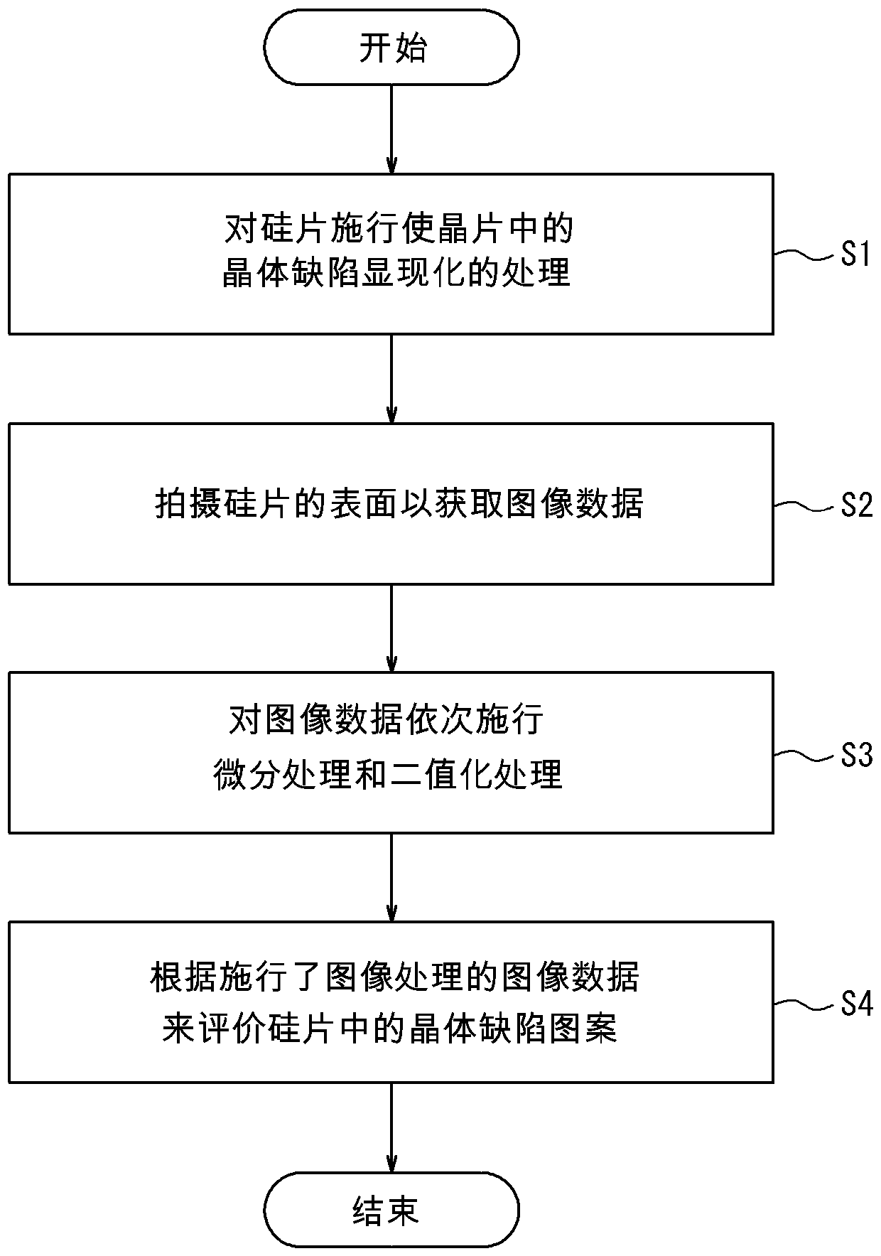
[0104] First, by the CZ method, a single crystal silicon ingot having a diameter of 300 mm in a COP occurrence region was grown. Secondly, wafer processing was performed on the grown silicon ingot to obtain a silicon wafer (thickness: 1 mm, resistivity: 10-12 Ω·cm, oxygen concentration: 9-13×10 17 atoms / cm 3 (ASTM F121 1979)). The above-mentioned silicon wafer was subjected to acid-based chemical etching treatment and cleaned, and then copper decoration treatment was performed. Then, a silicon wafer was etched using Wright's solution to obtain a sample.
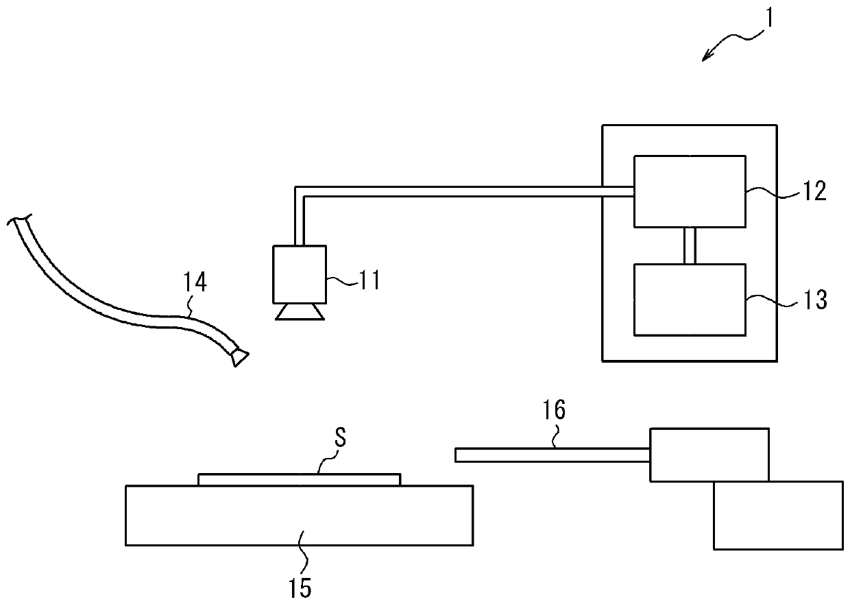
[0105] Next, the sample obtained in the above manner was scanned using a line scan camera (manufactured by DALSA, model: P2-2X-04K40) to obtain a one-dimensional image, and the obtained one-dimensional images were connected to obtain a two-dimensional image of 256 levels.
[0106] Next, differential processing (Sobel) and binarization processing (threshold value: 40) were performed on the im...
example 1
[0111] Similar to Invention Example 1, crystal defects in samples of silicon wafers were evaluated. However, image capture to image processing were not carried out, but the surface of the processed sample was visually observed by 5 measurers, and crystal defects were evaluated. Other conditions are exactly the same as Invention Example 1. The obtained results are shown in Table 1.
[0112] (Invention Example 2)
[0113] Similar to Invention Example 1, crystal defects in samples of silicon wafers were evaluated. However, silicon wafers are taken from single crystal silicon in the dislocation cluster region. Other conditions are exactly the same as Invention Example 1. The obtained results are shown in Table 1.
[0114] (existing example 2)
[0115] Similar to Conventional Example 1, crystal defects in samples of silicon wafers were evaluated. However, silicon wafers are taken from single crystal silicon in the dislocation cluster region. Other conditions are exactly the s...
PUM
| Property | Measurement | Unit |
|---|---|---|
| diameter | aaaaa | aaaaa |
| thickness | aaaaa | aaaaa |
| electrical resistivity | aaaaa | aaaaa |
Abstract
Description
Claims
Application Information


