Parallel mode converter and optical divider composed by the same

A technology of mode conversion and optical splitter, applied in the direction of light guide, optics, instrument, etc., to achieve the effect of reducing additional loss

Active Publication Date: 2008-12-10
李冰
View PDF0 Cites 17 Cited by
  • Summary
  • Abstract
  • Description
  • Claims
  • Application Information

AI Technical Summary

Problems solved by technology

However, in planar optical integrated circuits based on SOI or other high material refractive index cont

Method used


Image

  • Parallel mode converter and optical divider composed by the same
  • Parallel mode converter and optical divider composed by the same
  • Parallel mode converter and optical divider composed by the same

Examples


Example Embodiment

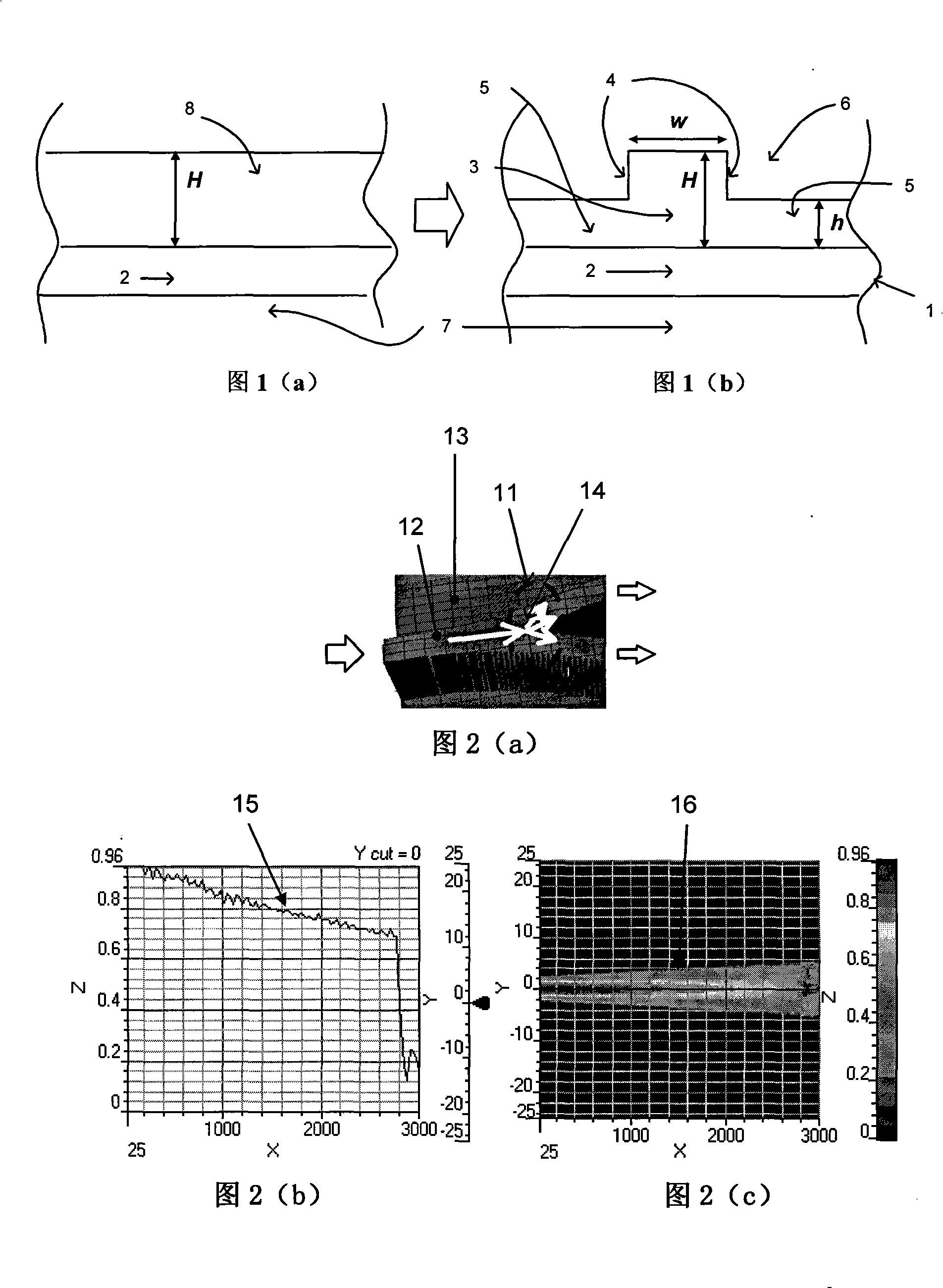
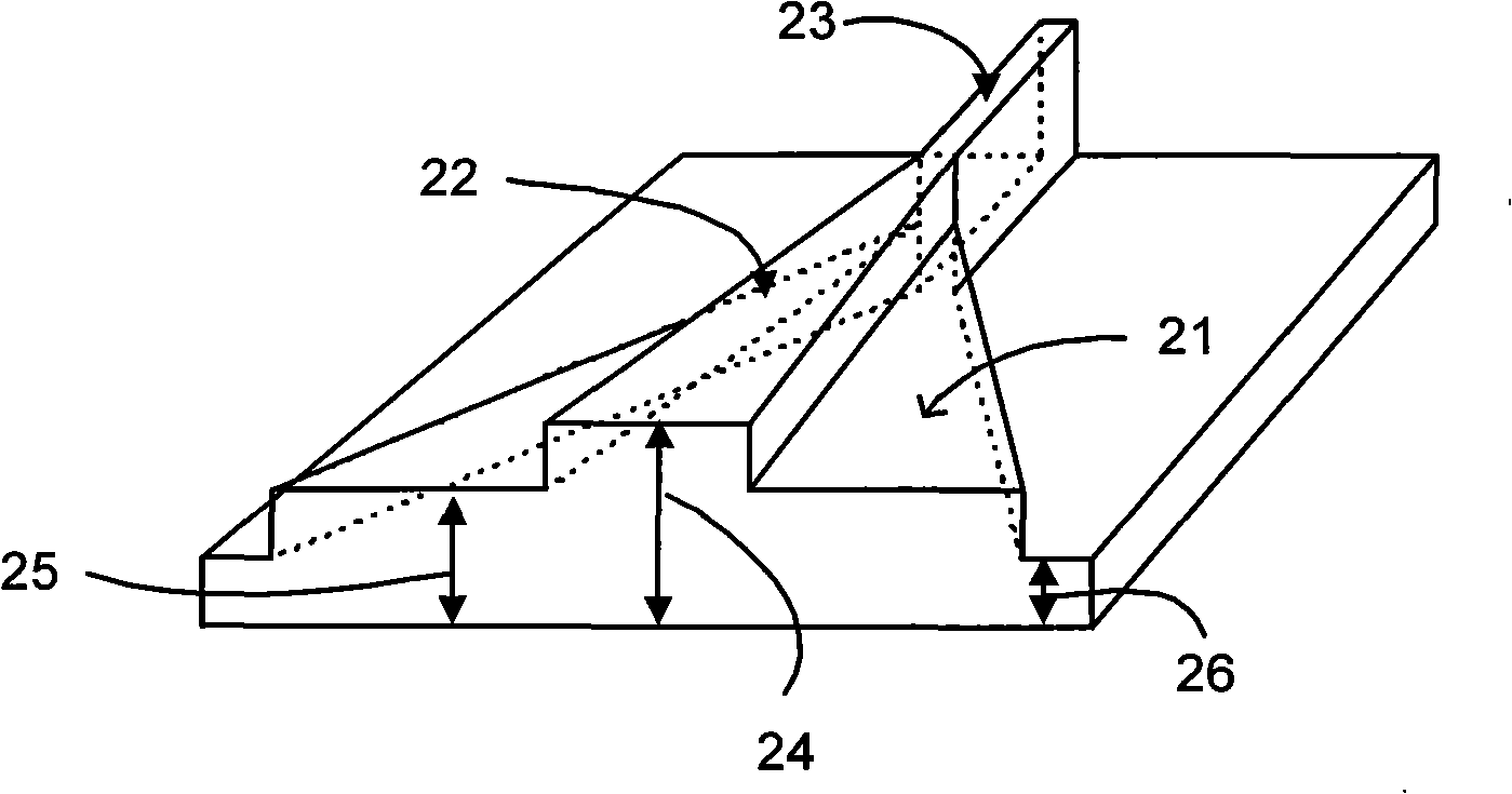
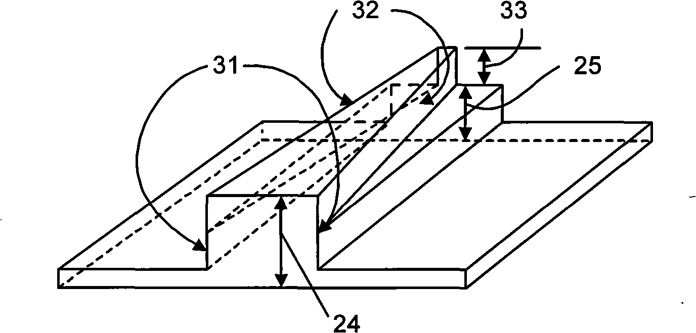
[0031] we use image 3 Explain the waveguide structure formed by deep and shallow two-step etching, image 3 It is a schematic diagram of the mode conversion structure between different ridge waveguides formed for deep etching and shallow etching. In the figure: the starting silicon plate 24 starts from the SOI wafer; the shallow etching is performed on it to form the ridge waveguide 22, which is The width of the waveguide ridge is wide in the front and narrow in the back; after the shallow etching, there are high-level slab areas 25 on both sides of the waveguide ridge; deep etching forms a deeply etched ridge waveguide 23 connected to the back of the shallow etched ridge waveguide 22, and at the same time limits the shallow etched ridge waveguide The lateral dimension of the high-level slab area on both sides of 22, this limited high-level slab area is referred to as the shoulder 21 here; the shoulder 21 and the deep-etched ridge waveguide 23 are on both sides of the low-level...


PUM


Abstract

The invention discloses a parallel model converter and a light splitter composed of the same, the solved technical issue is about reduction of optical field loss at a split location of the light splitter in SPI integrated optical loop. The inventive parallel mode converter has parallel multi-paths waveguide ridges distributed on an optical planar waveguide, each parallel multi-paths waveguide ridge is gradually widened in width of ridge waveguide from an input end to an output end. The light splitter is formed by sequentially connecting an incident coupling light waveguide, a single-channel mode converter, a lateral free propagation region and a mode converter, the optical planar waveguide of the mode converter is provided with the parallel multi-paths waveguide ridges the width of which is gradually widened from the input end to the output end. Compared with the prior art, the invention has the structure of parallel multi-paths waveguide ridges the width of which is gradually widened from the input end to the output end, which lowers scattering loss at the split location, and the light wave can avoid from being scattered by silicon dioxide between silicon channels in the process of conversion.

Description

technical field [0001] The invention relates to an integrated optoelectronic device, in particular to a mode converter and a low-loss optical splitter composed of it. Background technique [0002] Optical waveguides and planar optical integrated circuit PLCs based on silicon SOI on insulating substrates can help reduce the cost of optical chips and realize multifunctional monolithic integration. However, in planar optical integrated circuits based on SOI or other high material refractive index contrast substrates, the scattering loss at the branch junction is an obstacle to construct low-loss devices. The extra loss of a general-purpose silicon dioxide-based optical splitter is less than 0.5dB, while the extra loss of a typical SOI optical splitter is greater than 1dB. The large branch junction loss is due to the high material refractive index contrast direct result. [0003] Figure 1 is a schematic cross-sectional view of an SOI ridge waveguide. Fig. 1 (a) is initial SOI...

Claims


Application Information

Patent Timeline
IPC IPC(8): G02B6/122G02B6/125H04B10/12
Inventor 李冰
Owner 李冰
Why Eureka
Try Eureka