Organic solar cell based on triangular prism grating imprinting and production method thereof

A technology of solar cells and triangular prisms, applied in photovoltaic power generation, circuits, electrical components, etc., can solve the problems of low photogenerated carrier transfer efficiency and lower device performance, and achieve the goal of ensuring absorption, improving device performance, and increasing short-circuit current Effect

Pending Publication Date: 2021-11-12
UNIV OF ELECTRONIC SCI & TECH OF CHINA +1
View PDF5 Cites 0 Cited by
  • Summary
  • Abstract
  • Description
  • Claims
  • Application Information

AI Technical Summary

Problems solved by technology

[0004] The purpose of the present invention is to provide an organic solar cell based on triangular prism grating imprinting and its preparation method, aiming to solve the problem of photogenerated carriers caused by poor phase separation of the active layer in bulk heterojunction organic solar cell devices The low efficiency of separation, transport and interfacial transfer will eventually reduce the performance of the device, and at the same time, eliminate the negative impact of the use of orthogonal solvents on the compatibility of the active layer and device performance in the traditional continuous wet deposition process

Method used


Image

  • Organic solar cell based on triangular prism grating imprinting and production method thereof

Examples


Embodiment 1

[0036] Embodiment 1 (control group):

[0037] 1. Clean the substrate composed of transparent substrate and transparent conductive cathode ITO with surface roughness less than 1nm, and dry it with nitrogen after cleaning;

[0038] 2. Spin-coat PEDOT:PSS (3000rpm, 60s, 40nm) on the surface of the transparent conductive cathode ITO to prepare the anode buffer layer, and perform thermal annealing on the formed film (150°C, 1h);

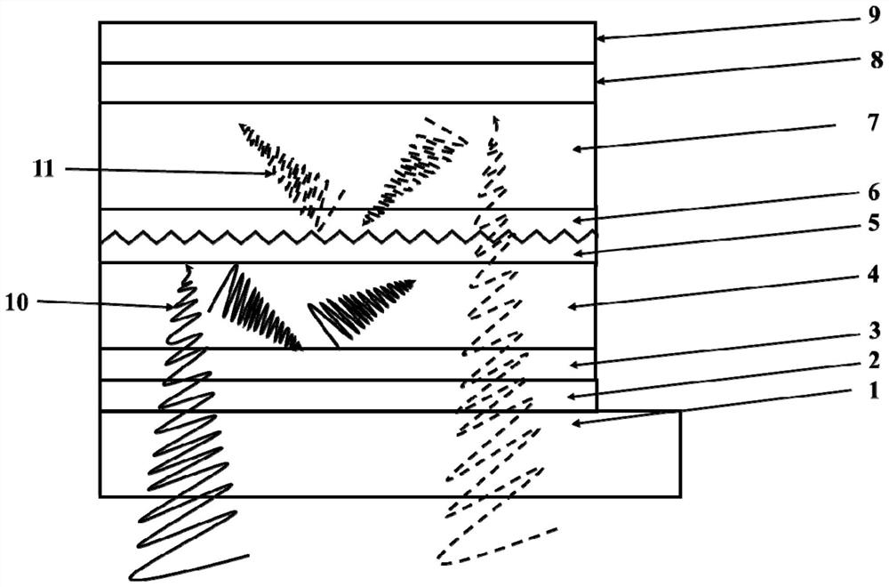
[0039] 3. Connect PBDB-T:PC 71 After the BM solution was dripped on the center of the PEDOT:PSS anode buffer layer, the active layer 4 of the top cell was prepared by a spin coating process (2000rpm, 60s, 80nm), and annealed (100°C, 30min);

[0040] 4. After the ZnO NPs dispersion liquid is drop-coated on the center of the active layer 4 of the top cell, a ZnONPs cathode buffer layer (3000rpm, 40s, 50nm) is prepared by a spin coating process, and annealed;

[0041] 5. After dropping the PEDOT:PSS precursor solution on the ZnO NPs cathode buffer layer, the...

Embodiment 2

[0047] 1. Clean the substrate composed of transparent substrate and transparent conductive cathode ITO with surface roughness less than 1nm, and dry it with nitrogen after cleaning;

[0048] 2. Spin-coat PEDOT:PSS (3000rpm, 60s, 40nm) on the surface of the transparent conductive cathode ITO to prepare the anode buffer layer, and perform thermal annealing on the formed film (150°C, 1h);

[0049] 3. Connect PBDB-T:PC 71 After the BM solution was dripped on the center of the PEDOT:PSS anode buffer layer, the active layer 4 of the top cell was prepared by a spin coating process (2000rpm, 60s, 80nm), and annealed (100°C, 30min);

[0050] 4. After the ZnO NPs dispersion liquid is drop-coated on the center of the active layer 4 of the top cell, a ZnONPs cathode buffer layer (3000rpm, 40s, 50nm) is prepared by a spin coating process, and annealed;

[0051] 5. Use a triangular prism nanoimprint plate (width: 0.3um, height: 30nm) to imprint the ZnO NPs cathode buffer layer to prepare a...

Embodiment 3

[0058] 1. Clean the substrate composed of transparent substrate and transparent conductive cathode ITO with surface roughness less than 1nm, and dry it with nitrogen after cleaning;

[0059] 2. Spin-coat PEDOT:PSS (3000rpm, 60s, 40nm) on the surface of the transparent conductive cathode ITO to prepare the anode buffer layer, and perform thermal annealing on the formed film (150°C, 1h);

[0060] 3. Connect PBDB-T:PC 71 After the BM solution was dripped on the center of the PEDOT:PSS anode buffer layer, the active layer 4 of the top cell was prepared by a spin coating process (2000rpm, 60s, 80nm), and annealed (100°C, 30min);

[0061] 4. After the ZnO NPs dispersion liquid is drop-coated on the center of the active layer 4 of the top cell, a ZnONPs cathode buffer layer (3000rpm, 40s, 50nm) is prepared by a spin coating process, and annealed;

[0062] 5. Use a triangular prism nanoimprint plate (width: 1um, height: 50nm) to imprint the ZnO NPs cathode buffer layer to prepare a Z...


PUM

PropertyMeasurementUnit
Concentrationaaaaaaaaaa
Thicknessaaaaaaaaaa
Thicknessaaaaaaaaaa

Abstract

The invention discloses an organic solar cell based on triangular prism grating imprinting and a production method thereof, and belongs to the field of organic semiconductor thin film solar cells. The laminated organic solar cell provided by the invention adopts an inversion structure and sequentially comprises a substrate, a transparent conductive cathode, a first anode buffer layer, a top cell active layer, a triangular prism grating type cathode buffer layer, a second anode buffer layer, a bottom cell active layer, a cathode buffer layer and a metal cathode from bottom to top. According to the nano-imprinting process based on the triangular prism type grating, the triangular prism type nano-imprinting plates of different specifications are selected to perform imprint processing on the triangular prism type grating cathode buffer layer so that the triangular prism type grating cathode buffer layer has the special optical characteristics of the triangular prism configuration, and the absorption of a laminated device to light waves of different wave bands is improved. According to the method, different reflection effects of the triangular prism grating on light waves with different wavelengths are effectively utilized, and the overall device performance of the laminated device is improved.

Description

technical field [0001] The invention belongs to the field of organic polymer photovoltaic devices or organic semiconductor thin film solar cells, and relates to an organic solar cell based on triangular prism grating imprinting and a preparation method thereof. Background technique [0002] In the past ten years, thanks to the emergence of new electron donor and electron acceptor materials, as well as the in-depth exploration of corresponding device engineering, interface engineering and other research work, organic solar cells have developed rapidly. Among them, the energy conversion efficiency of organic solar cell devices with fullerene derivative acceptors has reached more than 13%, while the performance of organic solar cell devices based on non-fullerene acceptors has exceeded 17%. However, compared with other photovoltaic technologies (such as: silicon-based, GaAs, perovskite, etc.), the current organic solar cells still need further improvement, among them, the light...

Claims


Application Information

Patent Timeline
IPC IPC(8): H01L51/42H01L51/44H01L51/46H01L51/48
CPCH10K85/215H10K30/87H10K30/81H10K30/30Y02E10/549
Inventor 于军胜张大勇王瑞李嘉文
Owner UNIV OF ELECTRONIC SCI & TECH OF CHINA
Why Eureka
Try Eureka