Method for bonding between electrical devices using ultrasonic vibration

A technology of electrical devices and ultrasonic waves, which is applied in the field of bonding between electrical devices, can solve problems such as difficult ACF bonding processes, and achieve the effect of reducing processing pressure and increasing production

Active Publication Date: 2008-12-10
KOREA ADVANCED INST OF SCI & TECH
View PDF0 Cites 20 Cited by
  • Summary
  • Abstract
  • Description
  • Claims
  • Application Information

AI Technical Summary

Problems solved by technology

Especially, if the thickness of the compound semiconductor chip or the silicon chip is thin, such as relatively fragile by processing pressure, it is difficult to implement the ACF bonding process due to the limitation of the bonding pressure generated

Method used


Image

  • Method for bonding between electrical devices using ultrasonic vibration
  • Method for bonding between electrical devices using ultrasonic vibration
  • Method for bonding between electrical devices using ultrasonic vibration

Examples


Embodiment Construction

[0034] The present invention will be described in detail below.

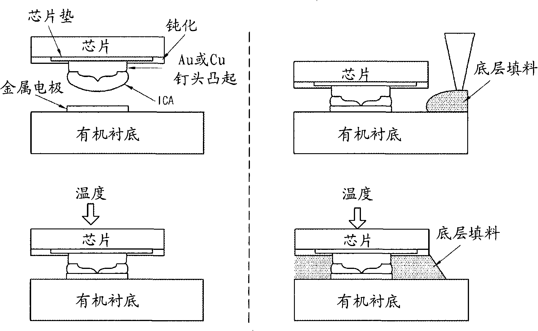
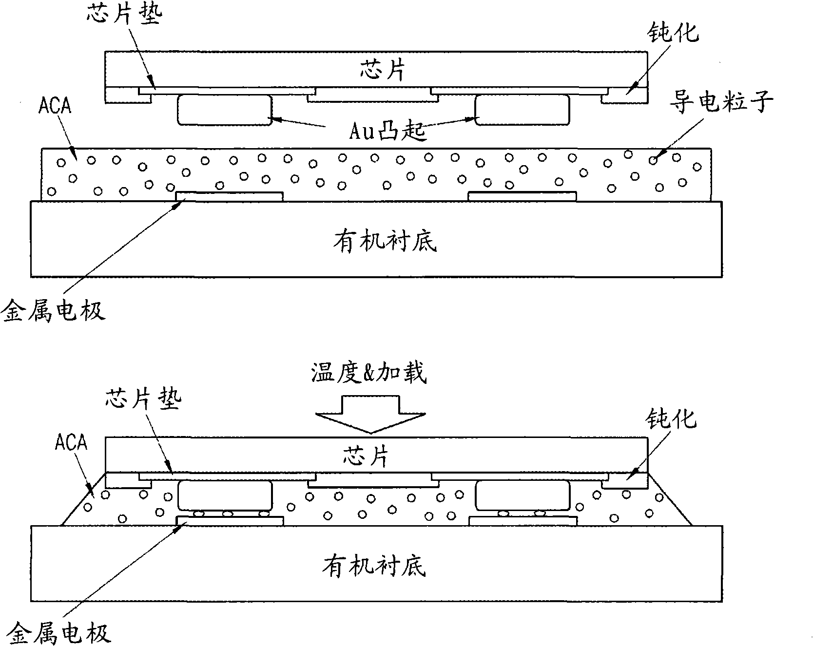
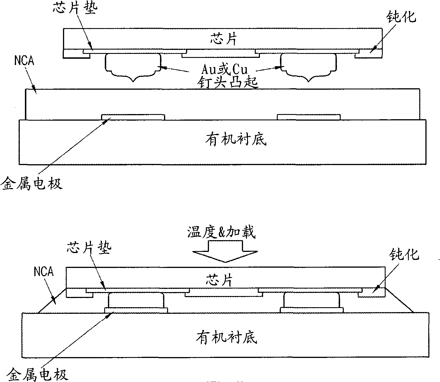
[0035] In the present invention, an electrical device to be bonded means a device used in an electrical product such as a semiconductor chip or a substrate, and bonding between an electrical device means between a semiconductor chip and a substrate, a semiconductor chip and a An electrical connection between semiconductor chips or between a substrate and a substrate.

[0036] The type of such semiconductor chips is not particularly limited, and may include, for example, display driver circuit ICs, image sensor ICs, memory ICs, non-memory ICs, ultra-high frequency or RF ICs, semiconductor ICs with silicon as a main component, and compound semiconductor ICs.

[0037] In electrodes on the bonding area (or input / output pads), the semiconductor chip may have no non-solder bumps or may have bumps selected from, for example, gold stud bumps, copper stud bumps, gold plated bumps, copper plated One of bumps, electroless...


PUM


Abstract

The present invention is to provide a method for bonding between electrical devices, including the steps of: aligning electrodes on a bonded area of an upper electrical device and a lower electrical device to be bonded; and curing of adhesives by applying ultrasonic energy to the adhesives between the upper electrical device and the lower electrical device.

Description

technical field [0001] The present invention relates to a method of bonding between electrical devices, and more particularly to a method of bonding between electrical devices which, when bonded between electrical devices, enables There is no need to apply heat from the outside or relatively low-temperature heat in the process of curing the adhesive, and the processing pressure in the case of the thermocompression bonding process is reduced. Background technique [0002] With the current demand for semiconductor packaging processes such as slim and light, high performance, high integration and environmental protection, the importance of the flip chip process is highlighted in the chip level bonding method. The flip-chip process is currently expanding its use to display packaging, such as smart cards, LCDs, PDPs, etc., computers, mobile phones, and communication systems. The interconnect materials used in the flip chip process can be broadly classified into solder and non-so...

Claims


Application Information

Patent Timeline
IPC IPC(8): H01L21/60
CPCH01L24/29H01L24/45H01L24/83H01L24/90H01L2224/1134H01L2224/13099H01L2224/13144H01L2224/13147H01L2224/1319H01L2224/16225H01L2224/293H01L2224/29399H01L2224/45124H01L2224/45144H01L2224/45147H01L2224/83192H01L2224/838H01L2924/01005H01L2924/01013H01L2924/01014H01L2924/01022H01L2924/01029H01L2924/0103H01L2924/01033H01L2924/01046H01L2924/01047H01L2924/0105H01L2924/01059H01L2924/01078H01L2924/01079H01L2924/01082H01L2924/0781H01L2924/09701H01L2924/14H01L2224/2919H01L2224/32225H01L2224/73204H01L2924/01006H01L2924/01076H01L2924/01087H01L2924/014H01L2924/0665H01L2224/29101H01L2924/0132H01L2924/01028H01L2224/2929H01L2224/83851H01L2924/10253H01L2924/00014H01L2924/07811H01L24/11H01L24/13H01L2924/07802H01L2924/15788H01L2924/12044H01L2224/11H01L2224/13H01L2224/05567H01L2224/05573H01L2924/00H01L2924/00012H01L2224/48H01L2224/05599H01L21/52
Inventor 白京煜任明镇金亨俊李技元
Owner KOREA ADVANCED INST OF SCI & TECH
Why Eureka
Try Eureka