
Light dope ion injection method

An ion implantation and light doping technology, applied in electrical components, semiconductor/solid-state device manufacturing, circuits, etc., can solve problems such as affecting the process, and achieve the effect of enhancing implantation diffusion and suppressing hot carrier effects

Inactive Publication Date: 2008-12-24
SEMICON MFG INT (SHANGHAI) CORP
View PDF1 Cites 5 Cited by
  • Summary
  • Abstract
  • Description
  • Claims
  • Application Information

AI Technical Summary

Problems solved by technology

However, when this method is used to suppress the hot carrier effect, the structure of the gate oxide layer will be changed, which will affect the subsequent process.

Method used


Image

  • Light dope ion injection method
  • Light dope ion injection method
  • Light dope ion injection method

Examples


Embodiment Construction

[0028] Although the invention will be described in more detail below with reference to the accompanying drawings, in which preferred embodiments of the invention are shown, it should be understood that those skilled in the art can modify the invention described herein and still achieve the advantageous effects of the invention. Therefore, the following description should be understood as a broad instruction for those skilled in the art, rather than as a limitation of the present invention.

[0029] In the interest of clarity, not all features of an actual implementation are described. In the following description, well-known functions and constructions are not described in detail since they would obscure the invention with unnecessary detail. It should be appreciated that in the development of any actual embodiment, numerous implementation details must be worked out to achieve the developer's specific goals, such as changing from one embodiment to another in accordance with sy...


PUM


Abstract

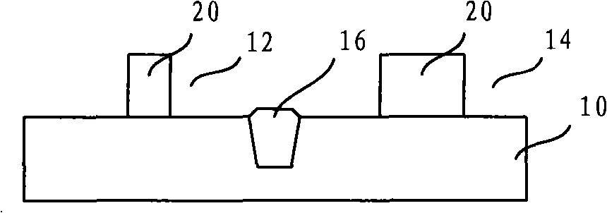
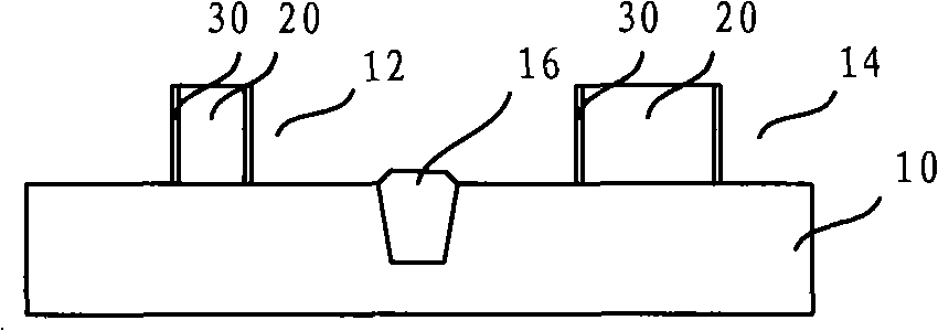
The invention relates to a light doping ion injecting method which comprises the following steps of: providing a semiconductor substrate which comprises a core device area and an input and output device area; forming a grid on the semiconductor substrate; implementing the light doping ion injecting to the input and output device area; forming a side wall substrate at the side wall of the grid; and implementing the light doping ion injecting to the core device area. The method can reduce the occurrence of hot-carrier effect.

Description

technical field [0001] The invention relates to the technical field of integrated circuit manufacturing, in particular to a lightly doped ion implantation method. Background technique [0002] The lightly doped ion implantation is used to form a lightly doped region, and the lightly doped region includes a lightly doped drain implantation (Lightly Doped Drain, LDD) region and a pocket (Pocket) ion implantation region, and the lightly doped region is used for It is used to define the source and drain extension regions of MOS devices. The LDD impurity is located below the gate and close to the edge of the channel region, and the Pocket impurity is located below the LDD region and close to the edge of the channel region, both of which provide impurity concentration gradients for the source and drain regions. [0003] Ion implantation is a standard technique for introducing conductivity-altering dopant materials into semiconductor substrates. In the ion implantation system, th...

Claims


Application Information

Patent Timeline
Patent Type & Authority Applications(China)
IPC IPC(8): H01L21/822H01L21/265
Inventor 李煜居建华
Owner SEMICON MFG INT (SHANGHAI) CORP
Learn More