Compound High Voltage Semiconductor Devices

A semiconductor and device technology, applied in the field of compound high-voltage semiconductor devices, can solve the problems of increased electric field, lower device reliability, and increased manufacturing costs, and achieve the effects of increasing junction depth, improving reliability, and reducing parasitic resistance

Active Publication Date: 2018-01-26
HANGZHOU SILAN MICROELECTRONICS
View PDF6 Cites 0 Cited by
  • Summary
  • Abstract
  • Description
  • Claims
  • Application Information

AI Technical Summary

Problems solved by technology

However, the disadvantage of this structure is that the potential of the P-type buried layer of this structure is floating, so that the P-type buried layer is not depleted when the device breaks down, and the electric field near the bird's beak becomes larger, thereby reducing the reliability of the device.
However, the disadvantages of this structure are as follows: first, the P buried layer is still a floating structure, and its disadvantages are similar to those of the device structure proposed by D.R. Disney et al. This increases the manufacturing cost

Method used


Image

  • Compound High Voltage Semiconductor Devices
  • Compound High Voltage Semiconductor Devices
  • Compound High Voltage Semiconductor Devices

Examples


no. 1 example

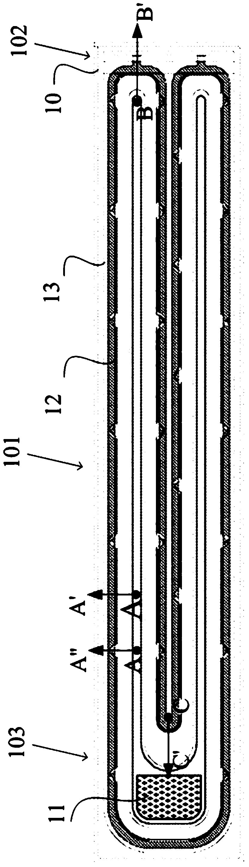
[0070] refer to figure 1 , figure 1 The layout structure of the composite high-voltage semiconductor device is shown, including a straight edge portion 101, a chamfered drain fingertip portion 102, and a chamfered source fingertip portion 103. The chamfered drain fingertip portion 102 and the source fingertip chamfered portion 103 are respectively Connect with straight side part 101. Wherein, the straight edge portion 101 is arranged along a straight line; the chamfered portion 102 of the drain fingertip and the chamfered portion 103 of the source fingertip are arranged in a curved manner, for example, the two may have appropriate chamfered shapes. Wherein, the straight side part 101 includes a plurality of straight side conductive parts and a plurality of straight side connecting parts spaced apart from each other, the area where the section line AA' is located is one of the straight side conductive parts, and the area where the section line AA" is located is A straight-edg...

no. 2 example

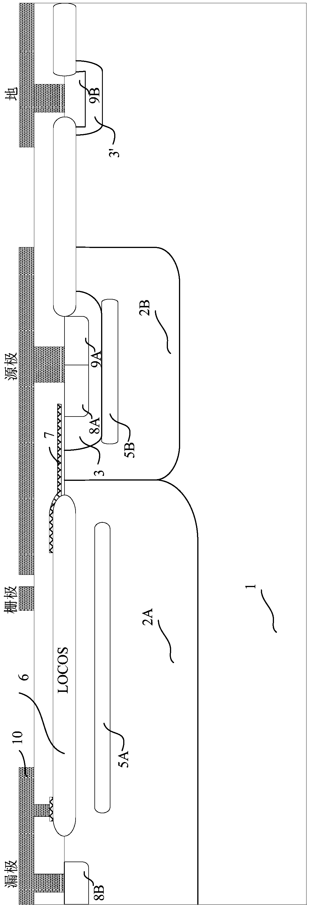
[0094] refer to Figure 7 , Figure 7 shows the cross-sectional structure of the straight-side conductive part of the compound high-voltage semiconductor device of the second embodiment, namely figure 1 The cross-sectional structure of the layout shown along the AA' direction, its structure is the same as figure 2 The structures shown are basically the same, the only difference is the doping type and figure 2 On the contrary, a P-type LDMOS structure is thus formed.

[0095] Correspondingly, the structure of the straight side connecting part is also the same as Figure 4 The same as shown, only the doping type of each doped region is reversed. For the chamfered portion of the source finger tip and the chamfered portion of the drain finger tip, the doping type of each doped region can be the same as that of the first embodiment (see Figure 5 and Figure 6 ) are the same, or vice versa.

no. 3 example

[0097] refer to Figure 8 , Figure 8 shows the cross-sectional structure of the straight-side conductive part of the composite high-voltage semiconductor device of the third embodiment, namely figure 1 The cross-sectional structure of the layout shown along the AA' direction, its structure is the same as figure 2 The structures shown are basically the same, the only difference is the doping type of the drain ohmic contact region 8B and figure 2 The illustrated embodiment is the opposite, that is, P-type doping, and the doping types of other doped regions are the same as figure 2 The illustrated embodiment is the same, resulting in a LIGBT device.

[0098] Correspondingly, the structure of the straight side connecting part is also the same as Figure 4 The same as shown, only the doping type of the drain ohmic contact region 8B is reversed. For the chamfered portion of the source finger tip and the chamfered portion of the drain finger tip, the doping type of each dope...


PUM


Abstract

The invention provides a composite high voltage semiconductor device; a layout comprises a straight edge portion arranged in a straight line; the straight edge portion comprises enhanced devices including the following: a semiconductor substrate; a first high voltage trap and a second high voltage trap arranged in parallel in the semiconductor substrate; a first field oxide layer arranged in the first high voltage trap; a first drain electrode ohmic contact zone arranged in the first high voltage trap of a first side of the first field oxide layer; a first source electrode ohmic contact zone arranged in the second high voltage trap; a first grid electrode at least covering the semiconductor substrate between the first source electrode ohmic contact zone and a second side of the first field oxide layer, wherein the first side of the first field oxide layer is far away from the second high voltage trap, and the second side of the first field oxide layer is close to the second high voltage trap. The doped concentration of the second high voltage trap is smaller than that of the first high voltage trap. The reliability of the device can be improved.

Description

technical field [0001] The invention relates to a semiconductor device, in particular to a composite high-voltage semiconductor device. Background technique [0002] BCD (Bipolar-CMOS-DMOS) technology is a monolithic integration process technology. This technology can make diodes (Bipolar), complementary metal-oxide-semiconductor field-effect transistors (CMOS) and double-diffused metal-oxide-semiconductor field-effect transistors (DMOS) devices on the same chip, so it is called BCD technology for short. [0003] High-voltage BCD technology generally refers to BCD technology with a withstand voltage of more than 100V. High-voltage BCD technology is currently widely used in AC-DC power supplies, LED drivers and other fields, and usually requires power devices with a withstand voltage ranging from 500V to 800V. [0004] Both LDMOS (lateral double diffusion MOS) devices and LIGBT (Lateral Insulated Gate Bipolar) devices are high-voltage lateral semiconductor devices, and are g...

Claims


Application Information

Patent Timeline
Patent Type & Authority Patents(China)
IPC IPC(8): H01L29/78H01L29/739H01L29/06H01L29/36
CPCH01L29/063H01L29/0684H01L29/36H01L29/7393H01L29/7816
Inventor 姚国亮张邵华吴建兴
Owner HANGZHOU SILAN MICROELECTRONICS
Why Eureka
Try Eureka