Self-aligning wafer or chip structure and self-aligning stacking structure and manufacturing method thereof

A technology of chip structure and manufacturing method, applied in semiconductor/solid-state device manufacturing, semiconductor/solid-state device components, semiconductor devices, etc., can solve time-consuming and other problems

Inactive Publication Date: 2008-12-24
IND TECH RES INST
View PDF2 Cites 7 Cited by
  • Summary
  • Abstract
  • Description
  • Claims
  • Application Information

AI Technical Summary

Problems solved by technology

In addition, the stacking methods currently proposed must go through one stacking and one reflow process to compl

Method used


Image

  • Self-aligning wafer or chip structure and self-aligning stacking structure and manufacturing method thereof
  • Self-aligning wafer or chip structure and self-aligning stacking structure and manufacturing method thereof
  • Self-aligning wafer or chip structure and self-aligning stacking structure and manufacturing method thereof

Examples


Embodiment Construction

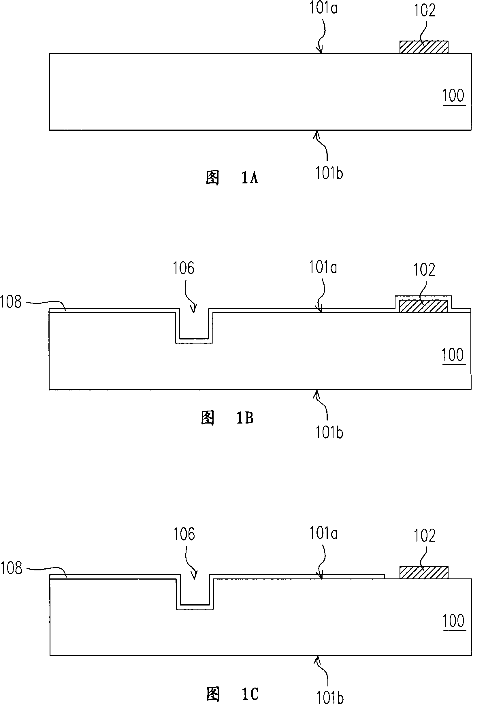
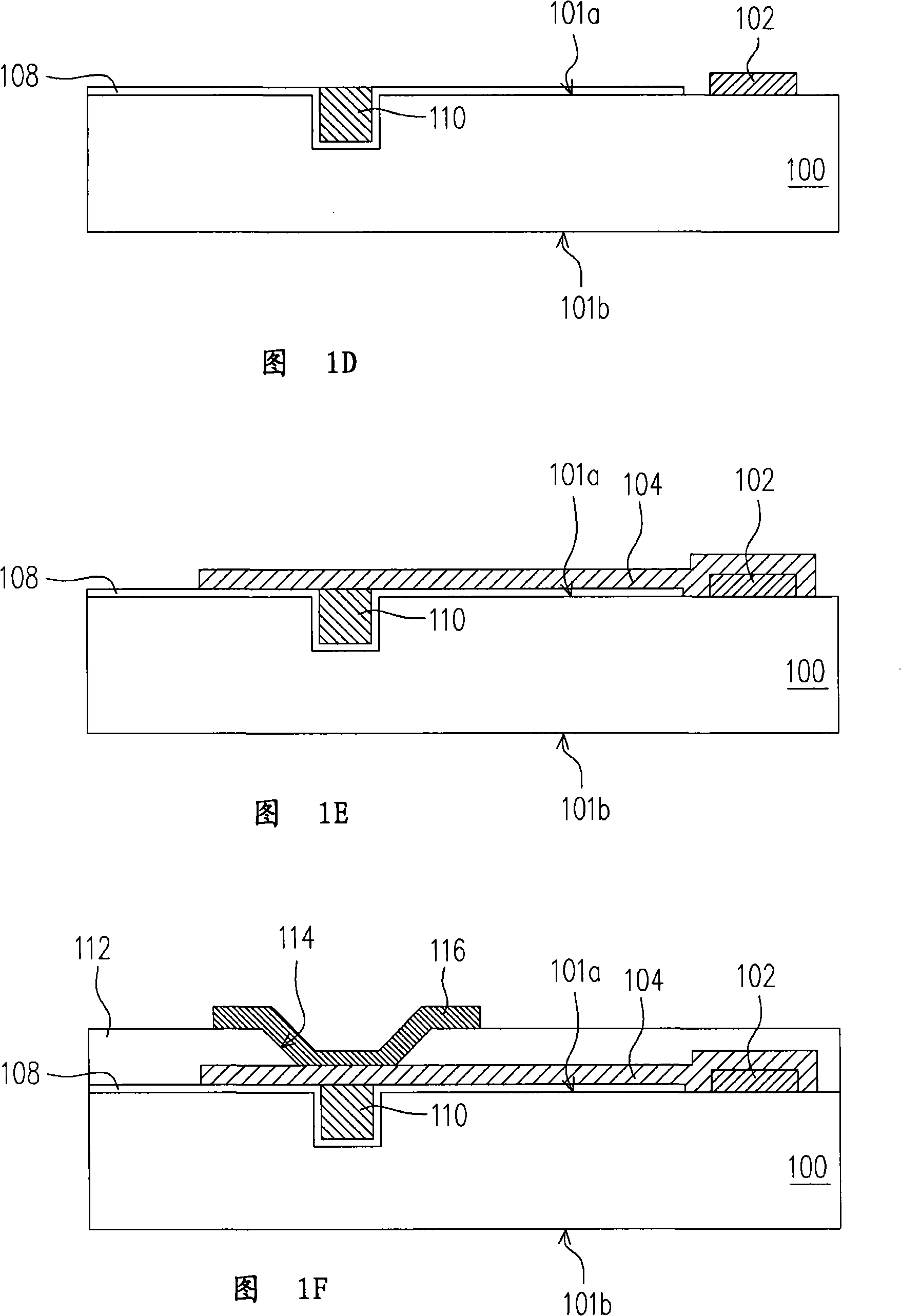
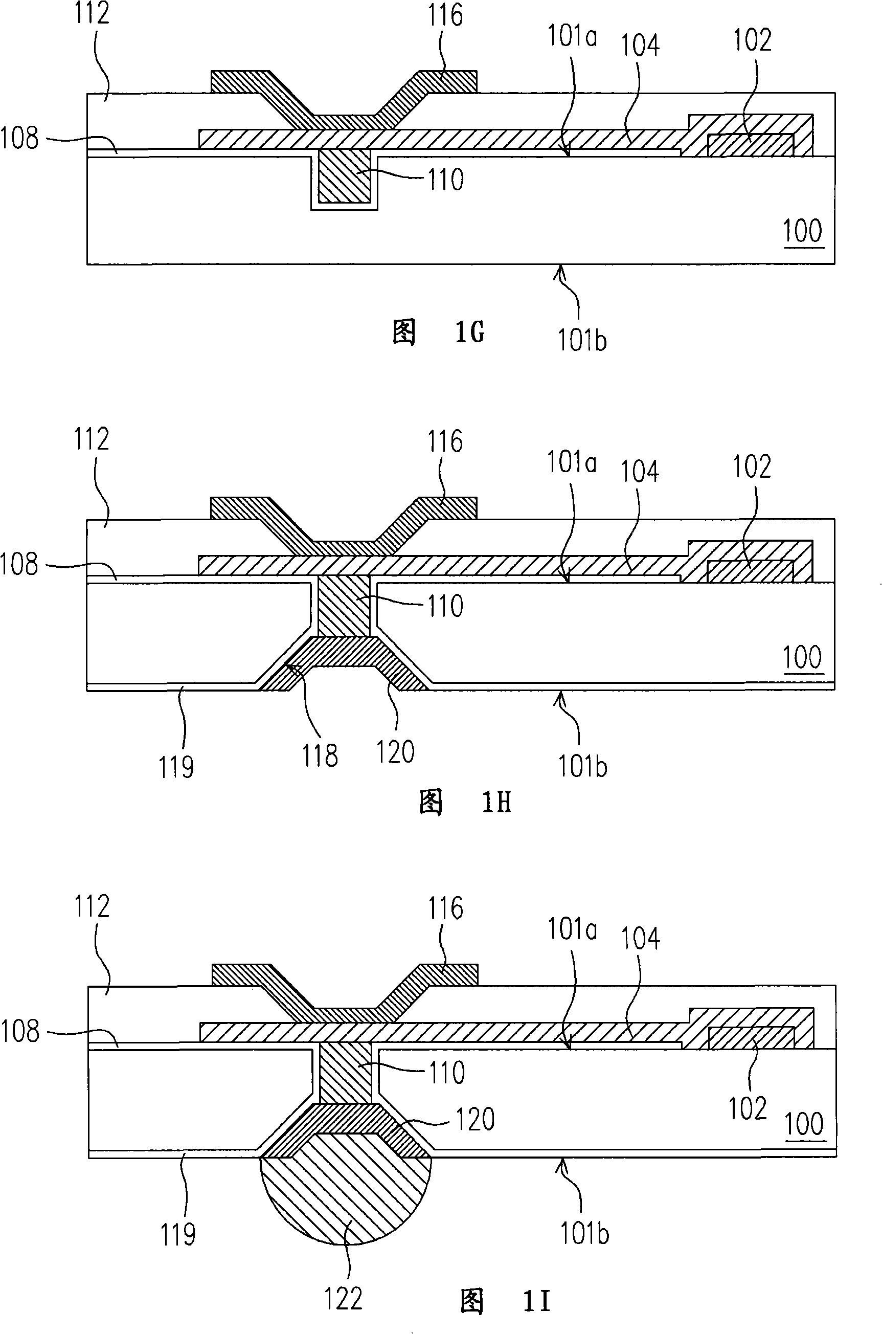
[0052] 1A to 1I are schematic cross-sectional views of a fabrication process of a self-aligned wafer or chip structure according to an embodiment of the present invention. Referring to FIG. 1A , firstly, a substrate 100 is provided, which has a first surface 101a and a second surface 101b. The substrate 100 is, for example, a wafer or a chip, and a plurality of elements and interconnection structures (not shown) have been formed in the substrate 100 . In particular, at least one solder pad 102 has been formed on the first surface 100 of the substrate 100 . The bonding pad 102 is electrically connected to the components and interconnection structures in the substrate 100 . The material of the pad 102 is, for example, metal. The bonding pad 102 is fabricated by using known deposition, photolithography and etching techniques, for example. In this embodiment, the bonding pad 102 is a bonding pad located at the center of the wafer or chip.

[0053] Next, please refer to FIG. 1B...


PUM


Abstract

The invention relates to a self-alignment chip or a chip structure, which comprises a substrate, at least a first recess, at least a second recess, at least a connecting structure and at least a lug. The substrate comprises a first surface and a second surface, and at least a pad is formed on the first surface. The first recess is positioned on the first surface, and the first recess is electrically connected with the pad. The second recess is arranged on the second surface. The connecting structure penetrates the substrate and is positioned between the first recess and the second recess, and the connecting structure is electrically connected with the first recess and the second recess. The lug can be filled in the second recess, and extend from the second surface.

Description

technical field [0001] The present invention relates to a wafer or chip structure and a stacked structure and a manufacturing method thereof, and in particular to a self-aligned (self-aligned) wafer or chip structure and a self-aligned stacked structure and a manufacturing method thereof . Background technique [0002] With the development of technology, more and more functions need to be integrated into a single application vehicle. The most obvious application vehicles are mobile phones that are most personal to individuals and memory card components that store a large amount of digital information. In addition, due to the inexhaustible demand of human beings for information bandwidth, more and more semiconductor components are designed in the direction of high frequency or ultra-high frequency, so the existing wire bonding technology can no longer meet the requirements. application of the above. [0003] At present, more and more structures are designed for high-densit...

Claims


Application Information

Patent Timeline
IPC IPC(8): H01L23/485H01L25/00H01L25/065H01L23/488H01L21/60
CPCH01L2224/16145
Inventor 陈荣泰何宗哲朱俊勋
Owner IND TECH RES INST
Why Eureka
Try Eureka