Gallium nitride transistor with self-aligned source and drain electrodes and preparation method of gallium nitride transistor

A source-drain electrode, gallium nitride technology, used in semiconductor/solid-state device manufacturing, circuits, electrical components, etc., can solve problems such as high manufacturing cost, increase, and limit device operating frequency

Pending Publication Date: 2020-10-27
XIDIAN UNIV
View PDF16 Cites 3 Cited by
  • Summary
  • Abstract
  • Description
  • Claims
  • Application Information

AI Technical Summary

Problems solved by technology

In conventional gallium nitride high electron mobility transistors, there is a certain distance between the gate and the source, and between the gate and the drain, which limits the reduction of the on-resistance of the transistor, thereby limiting the further improvement of the operating frequency of the device.
Existing technology that shortens the distance between the gate and the source and between the gate and the drain has disadvantages such as high manufacturing costs and large parasitics

Method used


Image

  • Gallium nitride transistor with self-aligned source and drain electrodes and preparation method of gallium nitride transistor
  • Gallium nitride transistor with self-aligned source and drain electrodes and preparation method of gallium nitride transistor
  • Gallium nitride transistor with self-aligned source and drain electrodes and preparation method of gallium nitride transistor

Examples


Embodiment 1

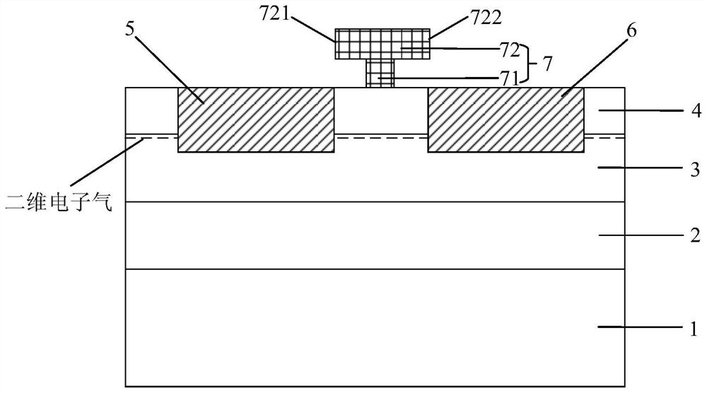
[0048] Please refer to figure 1 , figure 1 It is a structural schematic diagram of a gallium nitride transistor with self-aligned source-drain electrodes provided by an embodiment of the present invention. As shown in the figure, the gallium nitride transistor with self-aligned source-drain electrodes in this embodiment includes:

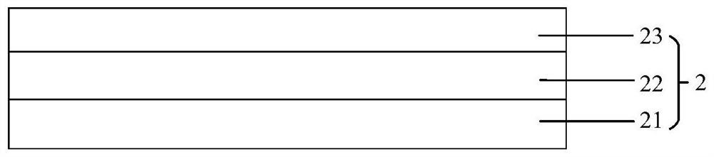
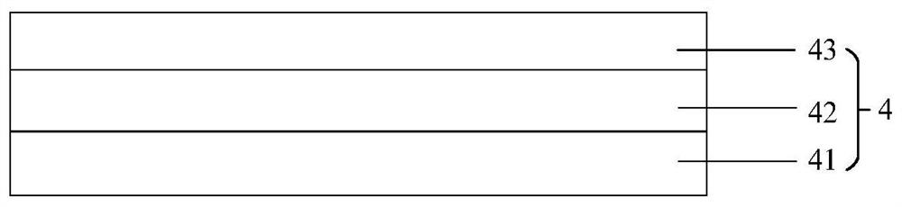
[0049] A substrate 1, a compound buffer zone 2, a channel layer 3 and a compound barrier region 4 are sequentially arranged from bottom to top, and there is a two-dimensional electron gas channel between the channel layer 3 and the compound barrier region 4;

[0050] The source electrode 5 is arranged inside the composite barrier region 4 and the channel layer 3;

[0051] The drain 6 is arranged inside the composite barrier region 4 and the channel layer 3, and is arranged at intervals from the source 5;

[0052] The gate 7 is arranged on the composite barrier region 4 and is located between the source 5 and the drain 6. The gate 7 includes a gate ...

Embodiment 2

[0077] See Figure 4 , Figure 4 It is a schematic flow chart of a method for preparing a gallium nitride transistor with self-aligned source-drain electrodes provided by an embodiment of the present invention. As shown in the figure, the method includes:

[0078] S100: continuously growing a compound buffer zone, a channel layer and a compound barrier region on the surface of the substrate;

[0079] Wherein, the composite buffer zone includes a nucleation layer, a transition layer and a buffer layer stacked in sequence, and the composite barrier region includes an isolation layer, a core barrier layer and a cap layer stacked in sequence.

[0080] S200: preparing a gate on the composite barrier region;

[0081] Wherein, the gate includes a grid foot and a grid head, the grid foot is located on the composite barrier region, the grid head is located on the grid foot, and the width of the grid head is greater than the width of the grid foot .

[0082] S300: Using the gate hea...


PUM

PropertyMeasurementUnit
thicknessaaaaaaaaaa
thicknessaaaaaaaaaa
thicknessaaaaaaaaaa

Abstract

The invention relates to a gallium nitride transistor with self-aligned source and drain electrodes and a preparation method of the gallium nitride transistor. The gallium nitride transistor with theself-aligned source and drain electrodes comprises a substrate, a composite buffer region, a channel layer, a composite barrier region, a source electrode, a drain electrode and a grid electrode, wherein the grid electrode comprises a grid pin and a grid head, and the width of the grid head is greater than that of the grid pin; the side surface, which is close to the grid electrode, of the sourceelectrode and the first side surface of the grid head are in the same vertical plane; the side surface, which is close to the grid electrode, of the drain electrode and the second side surface of thegrid head are in the same vertical plane. According to the gallium nitride transistor with the self-aligned source and drain electrodes, through self-alignment of the source electrode, the drain electrode and the grid electrode, a source-drain interval similar to the width size of the grid head is realized, the source-drain interval is reduced to the greatest extent, and the source electrode access resistance and the drain electrode access resistance of the transistor are reduced, so that the power loss of the transistor is reduced, and the frequency characteristic of the transistor is improved.

Description

technical field [0001] The invention belongs to the technical field of semiconductor devices, and in particular relates to a gallium nitride transistor with self-aligned source-drain electrodes and a preparation method thereof. Background technique [0002] Semiconductor radio frequency devices are widely used in communication technology, radar, satellite and so on. The semiconductor materials used for radio frequency devices mainly include the first-generation semiconductor silicon system materials, the second-generation semiconductor gallium arsenide / indium phosphide system materials, and the third-generation semiconductor gallium nitride-based materials. Among them, Gallium Nitride High Electron Mobility Transistor (HEMT, High Electron Mobility Transistor) has excellent performances such as high output power density, high efficiency, high temperature resistance, and radiation resistance. The core radio frequency device. [0003] With the further increase in the communic...

Claims


Application Information

Patent Timeline
Patent Type & Authority Applications(China)
IPC IPC(8): H01L29/778H01L21/335H01L29/417H01L29/423H01L29/20
CPCH01L29/778H01L29/66462H01L29/41725H01L29/42316H01L29/2003
Inventor 刘志宏王泽宇张进成朱肖肖宋昆璐周弘赵胜雷张雅超段小玲郝跃
Owner XIDIAN UNIV
Why Eureka
Try Eureka