Method for lowering contact resistance of two-dimensional material field effect transistor

A technology of field effect transistors and two-dimensional materials, which can be applied to circuits, electrical components, semiconductor devices, etc., and can solve problems such as limiting device performance

Inactive Publication Date: 2018-04-17
SUZHOU UNIV
View PDF1 Cites 3 Cited by
  • Summary
  • Abstract
  • Description
  • Claims
  • Application Information

AI Technical Summary

Problems solved by technology

[0003] However, the carrier mobility of currently reported 2D field-effect transistors is still much lower than the theoretical mobility of 2D materials themselves. One of the reasons is that the contact resistance between 2D materials and metal electrodes greatly limits the device performance
Therefore, how to effectively reduce the contact resistance between the two-dimensional material channel and the metal electrode is the main challenge faced by the application field of two-dimensional field effect transistors.

Method used


Image

  • Method for lowering contact resistance of two-dimensional material field effect transistor
  • Method for lowering contact resistance of two-dimensional material field effect transistor
  • Method for lowering contact resistance of two-dimensional material field effect transistor

Examples


Embodiment 1

[0054] see Figure 1-6 , this embodiment provides a method for reducing the contact resistance of a two-dimensional material field effect transistor, comprising the following steps:

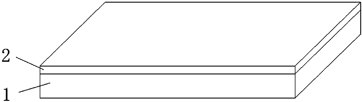
[0055] (1) Prepare the substrate, which is covered with silicon dioxide (SiO 2 ) P-type highly doped silicon wafer, the surface has 100nm thick SiO 2Layer 2 and Si layer 1 at the bottom were cleaned with acetone, ethanol, and deionized water respectively, and then the silicon wafer was blown dry with a nitrogen gun ( figure 1 ).

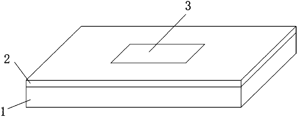
[0056] (2) Evaporate a rectangular transition metal region 3 on the upper surface of the substrate by electron beam evaporation, magnetron sputtering or atomic layer deposition, the area of ​​which is smaller than the area of ​​the upper surface of the substrate to form a transition metal layer with a thickness of 0.1 nm, the material is Mo( figure 2 ).

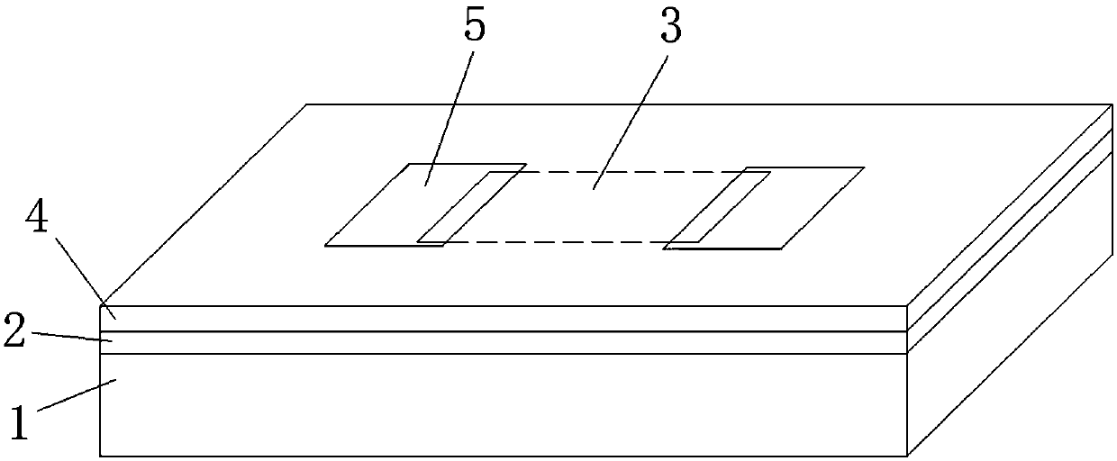
[0057] (3) spin-coating photoresist, followed by exposure and development to form a photoresist layer 4, which...

Embodiment 2

[0062] This embodiment provides a method for reducing the contact resistance of a two-dimensional material field effect transistor, including the following steps:

[0063] (1) Prepare the substrate, which is covered with silicon dioxide (SiO 2 ) P-type highly doped silicon wafer, the surface has 200nm thick SiO 2 Layers were cleaned with acetone, ethanol, and deionized water, and then the silicon wafer was blown dry with a nitrogen gun.

[0064] (2) Evaporate a rectangular transition metal region on the upper surface of the substrate by electron beam evaporation, magnetron sputtering or atomic layer deposition, the area of ​​which is smaller than the area of ​​the upper surface of the substrate to form a transition metal layer with a thickness of 0.1nm , the material is Mo.

[0065] (3) Spin-coat photoresist, followed by exposure and development to form a photoresist layer. There are two holes for evaporation source and drain electrodes on the photoresist layer. The holes ar...

Embodiment 3

[0070] This embodiment provides a method for reducing the contact resistance of a two-dimensional material field effect transistor, including the following steps:

[0071] (1) Prepare the substrate, which is covered with silicon dioxide (SiO 2 ) P-type highly doped silicon wafer, the surface has 250nm thick SiO 2 Layers were cleaned with acetone, ethanol, and deionized water, and then the silicon wafer was blown dry with a nitrogen gun.

[0072] (2) Evaporate a rectangular transition metal region on the upper surface of the substrate by electron beam evaporation, magnetron sputtering or atomic layer deposition, the area of ​​which is smaller than the area of ​​the upper surface of the substrate to form a transition metal layer with a thickness of 0.5nm , the material is Pt.

[0073] (3) Spin-coat photoresist, followed by exposure and development to form a photoresist layer. There are two holes for evaporation source and drain electrodes on the photoresist layer. The holes ar...


PUM


Abstract

The invention relates to a method for lowering contact resistance of a two-dimensional material field effect transistor. The method comprises the following steps of enabling at least one transitionalmetal region to be evaporated on the partial surface of a substrate to form a transitional metal layer, wherein the transitional metal region is 0.1-2nm in thickness; performing photoetching and developing to form a photoresist layer, wherein at least two holes for evaporating source and drain electrodes are formed in the photoresist layer, the downward side of each hole is just aligned to the partial transitional metal layer and the partial substrate surface, and each hole is positioned in one side of the transitional metal region separately; enabling the source and drain electrodes to be evaporated in the holes, and next, removing the photoresist layer to expose the other part of the substrate; and adopting a sulphur source to perform sulfuration on the transitional metal, or adopting aselenium source to perform selenylation of the transitional metal, and then performing cooling to form the two-dimensional material field effect transistor on the surface of the substrate. By adoptingthe source and drain electrodes as a protection isolation layer, a two-dimensional material channel is formed between the source and drain electrodes, so that the overlapped area between the channeland the source and drain electrodes is reduced, thereby lowering the contact resistance between the two parties.

Description

technical field [0001] The invention relates to the field of two-dimensional materials, in particular to a method for reducing the contact resistance of a two-dimensional material field effect transistor. Background technique [0002] As the active channel region of field effect transistors, semiconductor two-dimensional materials can overcome the short channel effect of traditional silicon-based field effect transistors. In addition, due to the ultra-thin thickness and excellent flexibility of two-dimensional materials, the preparation of ultra-small, bendable and flexible field-effect transistors can be realized based on two-dimensional materials. In recent years, based on two-dimensional MoS 2 、WS 2 、MoSe 2 、PtS 2 , PtSe 2 Field-effect transistors of semiconducting two-dimensional materials have attracted great attention. [0003] However, the carrier mobility of currently reported 2D field-effect transistors is still much lower than the theoretical mobility of 2D m...

Claims


Application Information

Patent Timeline
Patent Type & Authority Applications(China)
IPC IPC(8): H01L29/417H01L21/335
CPCH01L29/41725H01L29/66431
Inventor 李绍娟马玮良袁建孙甜拓明芬
Owner SUZHOU UNIV
Why Eureka
Try Eureka