

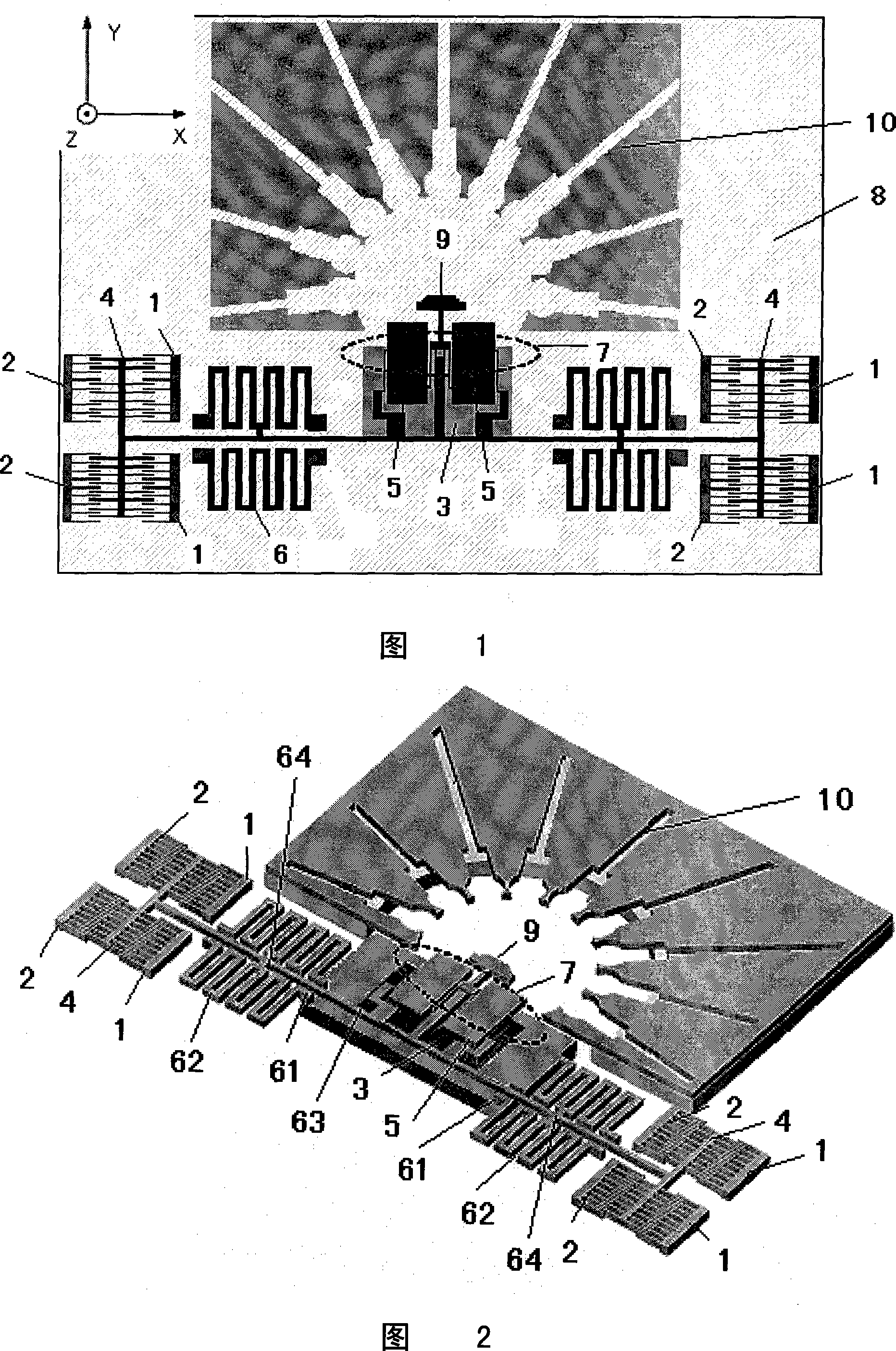
Minitype optical device and method for producing the same
An optical device and micro technology, applied in optical components, optics, opto-mechanical equipment, etc., can solve problems that are not conducive to the miniaturization of equipment, increase the difficulty of system maintenance, reduce system reliability, etc., to reduce difficulty and cost, and improve functions. Powerful, high-isolation effects
- Summary
- Abstract
- Description
- Claims
- Application Information
AI Technical Summary
Problems solved by technology
Method used
Image

Examples
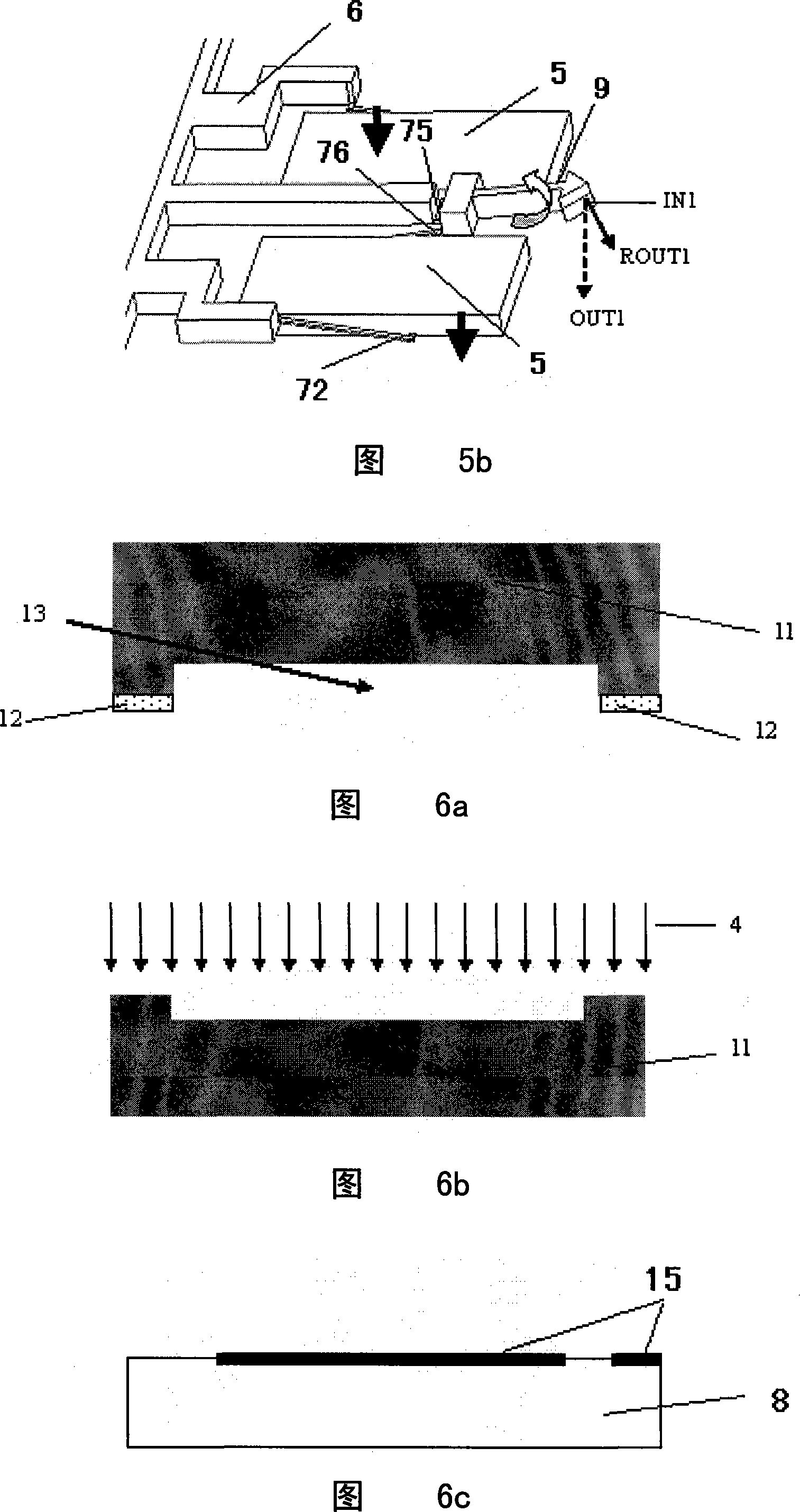
Embodiment 1
[0040] Embodiment 1: When making a micro-optical device with a single-ended unequal-height support beam, the following processes are mainly adopted:
[0041] 1. The starting material is a double-polished N-type (100) silicon wafer 11 (as shown in FIG. 6a ), with a thickness of 400±10 microns;
[0042] 2. Form a silicon oxide mask 12 on the silicon wafer 11, and then etch a deep groove 13. The depth of the deep groove 13 determines the gap between the fixed electrode 3 and the movable electrode 5 on the glass substrate;
[0043] 3. As shown in FIG. 6b, the silicon oxide mask 12 is removed, and the surface of the silicon wafer 11 is doped with boron 14 by ion implantation or diffusion process to form an ohmic contact;
[0044] 4. As shown in FIG. 6c, metal electrodes 15 are fabricated on the glass substrate 8 as lead electrodes of the micro-drive structure;
[0045] 5. As shown in FIG. 6d, the glass substrate 8 and the silicon wafer 11 are anodically bonded, and the silicon waf...
Embodiment 2
[0048] Embodiment 2: When making a micro-optical device with unequal-height support beams at both ends, the following processes are mainly used:
[0049] 1. The starting material is a double-polished N-type (100) silicon wafer 11 (as shown in FIG. 6a ), with a thickness of 400±10 microns;
[0050] 2. First, a silicon oxide mask 19 is formed on the silicon wafer 11, and then a photoresist mask 20 is formed on the surface of the silicon oxide mask 19 (as shown in FIG. 7 a ), and then a composite mask of silicon oxide and photoresist is formed. Then take the photoresist 20 as the mask etching deep groove 21 (as shown in Figure 7b), the depth of deep groove 21 determines the lower end of combined torsion beam 7 and folded beam 6 (comprising beams such as 71,72,73) height difference (as shown in Figure 7c);
[0051] 3. Remove the photoresist mask 20, and use the silicon oxide mask 19 as a mask to etch the silicon wafer 11 to form a deep groove 22. The depth of the deep groove 22 d...
PUM
| Property | Measurement | Unit |
|---|---|---|
| thickness | aaaaa | aaaaa |
Abstract
Description
Claims
Application Information