Vertical surrounding grid junction type field effect transistor, preparation method and applications thereof

A technology of field effect transistors and surrounding gates, which is applied in the field of sensors, can solve problems such as increasing process complexity, and achieve the effects of good process compatibility, simple process, and good technical compatibility

Inactive Publication Date: 2011-04-20
SHANGHAI INST OF MICROSYSTEM & INFORMATION TECH CHINESE ACAD OF SCI
View PDF0 Cites 0 Cited by
  • Summary
  • Abstract
  • Description
  • Claims
  • Application Information

AI Technical Summary

Problems solved by technology

Since the vibrating double-gate MOS transistor and the vibrating double-gate junction field effect transistor are both planar structures, it is generally necessary to make a vertical structure that is fixedly connected to the grid to achieve sensitivity to the lateral vibration of the sensitive structure, thereby significantly increasing the complexity of the process.

Method used


Image

  • Vertical surrounding grid junction type field effect transistor, preparation method and applications thereof
  • Vertical surrounding grid junction type field effect transistor, preparation method and applications thereof
  • Vertical surrounding grid junction type field effect transistor, preparation method and applications thereof

Examples


Embodiment 1

[0035] The manufacturing steps of the vertical surrounding gate junction field effect transistor provided by the present invention are:

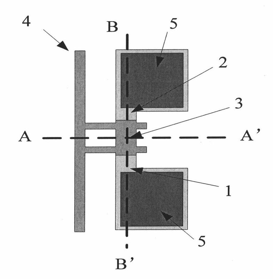
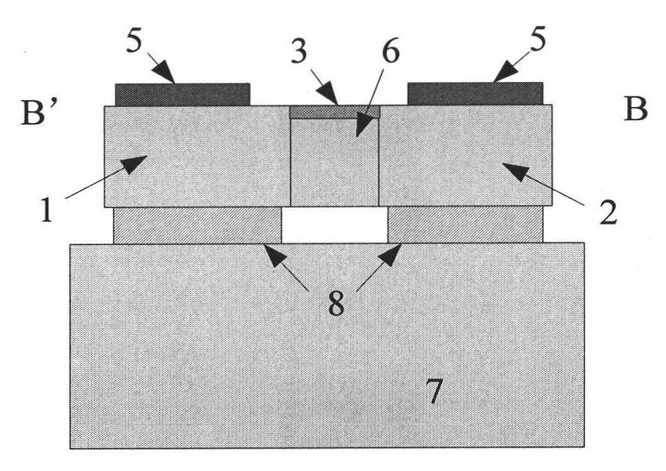
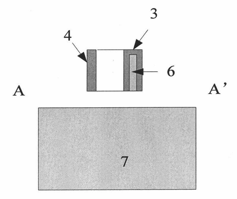
[0036] (1) For n-channel field-effect transistors, an SOI silicon wafer whose top layer silicon is n-type is used. A silicon oxide protective layer is thermally grown on top of the silicon. The sensitive structure, the sensitive gate, and the doped window surrounding the gate are etched by photolithography and dry etching process, and the oxide layer on the upper surface of the sensitive structure, the sensitive gate, and the upper surface of the surrounding gate is removed. Such as Figure 6 shown.

[0037] (2) Using the diffusion process of the integrated circuit, the upper surface and sidewall of the sensitive structure, the sensitive gate and the surrounding gate are doped. For n-channel field effect transistors, the doping type is p-type. For p-channel field effect transistors, the doping type is n-type. Doping concentrations up to...

Embodiment 2

[0042] Vertical surround-gate JFETs are offered for displacement detection of sensitive structures:

[0043] Fig. 10 shows a specific example of applying a vertical surrounding grid junction field effect transistor to a cantilever beam-mass structure acceleration sensor. In FIG. 10 , the detection of the displacement of the cantilever beam-mass structure in the plane of the silicon wafer is realized by using the vertical surrounding gate junction field effect transistor. The vertical surround gate field effect transistor can significantly reduce the influence of parasitic capacitance on displacement detection. The differential detection of the displacement of the cantilever beam-mass structure is realized by fabricating a vertical surrounding grid junction field effect transistor on both sides of the cantilever beam-mass structure. The cantilever beam-mass structure serves as the common grid of two vertically surrounding gate junction field effect transistors. The method of ...


PUM


Abstract

The invention relates to a vertical surrounding grid junction type field effect transistor, a preparation method and applications thereof. The field effect transistor comprises a source area, a drain area, a surrounding grid, a sensitive grid, a channel and a source-drain area press welding block or metal lead; wherein the source area and the drain area are connected through the channel; the sensitive grid and the surrounding grid are connected; the surrounding grid surrounds the upper surface, the left surface and the right surface of the channel which is vertical; the channel and the surrounding grid form a Pn junction; the source area and the drain area are electrically connected with an external circuit through the press welding block or the metal lead. The field effect transistor and a sensitive structure are manufactured on the top layer silicon of an SOI silicon chip and are simultaneously manufactured by adopting a micro-mechanical processing method. The displacement detection on the sensitive structure is realized through capacitance coupling.

Description

technical field [0001] The invention relates to a vertical surrounding gate junction type field effect transistor for sensor displacement detection, a manufacturing method and an application thereof, belonging to the field of sensors. Background technique [0002] Capacitance detection is a commonly used displacement detection technology in Micro-Electro-Mechanical-System (MEMS) (M.Bao, Micro Mechanical Transducers, Press: ELSEVIER, 2000.). A variety of micro-machined acceleration sensors and micro-machined gyroscopes use capacitance detection methods to achieve accurate measurement of the displacement of sensitive structures. With the increase of the integration degree and the decrease of the size of the MEMS integrated system, the capacitance value of the sensitive capacitor decreases accordingly. The sensitive capacitance value of the acceleration sensor made by the surface micromachine and SOI (Silicon on Insulator, silicon on insulator) micromachine technology is mostl...

Claims


Application Information

Patent Timeline
Patent Type & Authority Patents(China)
IPC IPC(8): H01L21/337G01B7/02B81B7/02H01L29/808B81C1/00
Inventor 杨恒成海涛戴斌吴燕红李昕欣王跃林
Owner SHANGHAI INST OF MICROSYSTEM & INFORMATION TECH CHINESE ACAD OF SCI
Why Eureka
Try Eureka