

Random memory and electricity supplying method thereof
A technology of random access memory and power supply method, which is applied in static memory, instruments, etc., can solve the problems of shortened storage unit data retention time, reduced sensitivity of sensitive amplifiers, and reduced stability of random access memory, etc., to improve the initial voltage difference and increase stability , The effect of increasing the data retention time
- Summary
- Abstract
- Description
- Claims
- Application Information
AI Technical Summary
Problems solved by technology
Method used
Image

Examples
Embodiment 1
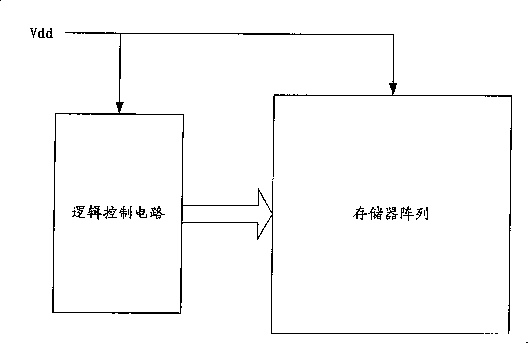
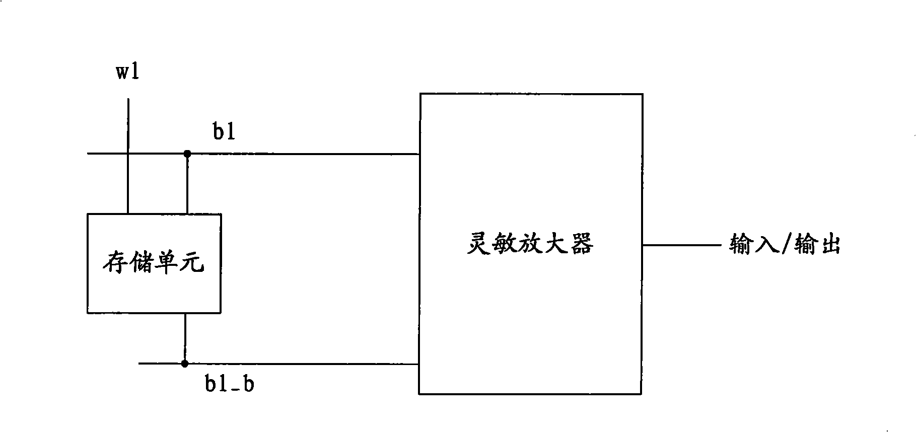
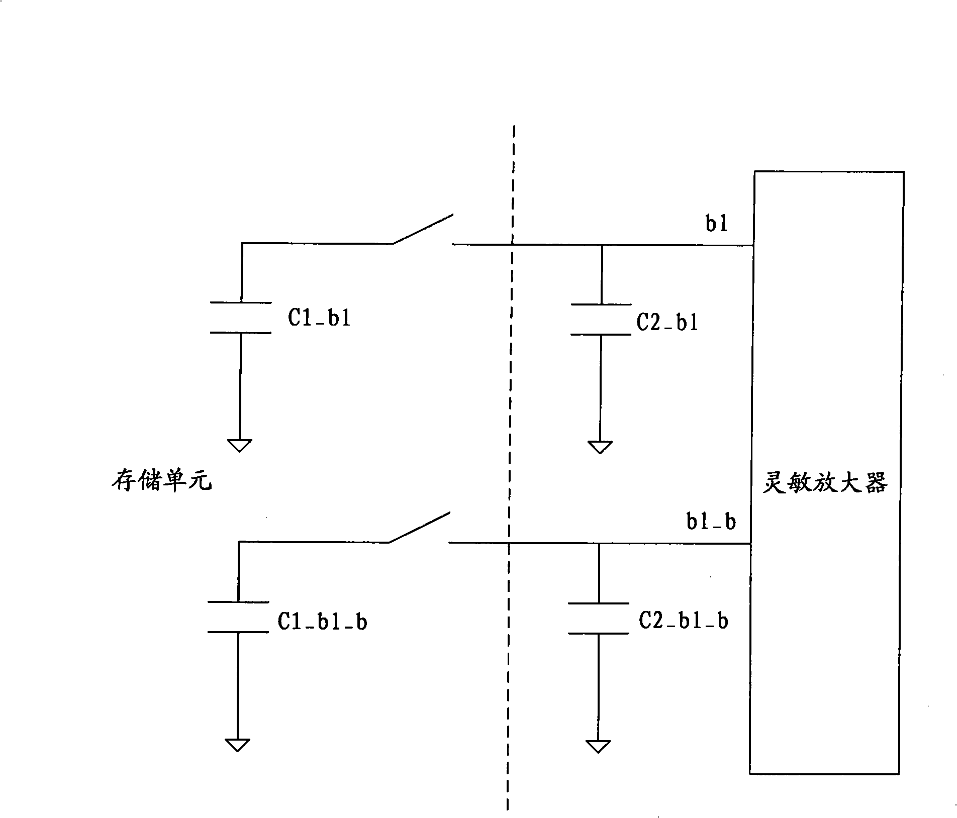
[0030] refer to Figure 4 The random access memory of this embodiment mainly includes: a logic control circuit 41, a memory array 42, a high-voltage charge pump 43, a voltage regulator 44, and the memory array 42 includes a memory cell array and a sense amplifier (not shown). Wherein, the logic control circuit 41 , the high-voltage charge pump 43 and the voltage regulator 44 are powered by the external power supply voltage Vdd. The high-voltage charge pump 43 converts Vdd to generate a voltage Vccs higher than Vdd, and uses the generated Vccs as the substrate bias voltage of the PMOS transistor of the memory cell array and the PMOS transistor of the sensitive amplifier; voltage regulator 44 Convert Vdd to generate a voltage Vcc higher than Vdd, and use the generated Vcc as the power supply voltage of the memory cell array and the sense amplifier.
[0031] It should be noted that how the high-voltage charge pump and the voltage regulator upgrade and convert the voltage is an e...
Embodiment 2
[0033] refer to Figure 5 , the random access memory of this embodiment mainly includes: a logic control circuit 51, a memory array 52, high-voltage charge pumps 53, 54, and the memory array 52 includes a memory cell array and a sense amplifier (not shown). Wherein, the logic control circuit 51 and the high-voltage charge pumps 53 and 54 are powered by the external power supply voltage Vdd. The high-voltage charge pump 53 converts Vdd to generate a voltage Vccs higher than Vdd, and uses the generated Vccs as the substrate bias voltage of the PMOS transistor of the memory cell array and the PMOS transistor of the sense amplifier; the high-voltage charge pump 54 Convert Vdd to generate a voltage Vcc higher than Vdd, and use the generated Vcc as the power supply voltage of the memory cell array and the sense amplifier.
[0034] In the second embodiment, there are two high-voltage charge pumps, which can also be realized by a separate high-voltage charge pump, that is, the extern...
Embodiment 3
[0037] refer to Figure 6, the random access memory of this embodiment mainly includes: a logic control circuit 61, a memory array 62, and a voltage generating module 63, and the memory array 62 includes a memory cell array and a sense amplifier (not shown). Wherein, the logic control circuit 61 and the voltage generation module 63 are powered by the external power supply voltage Vdd. The voltage generating module 63 converts Vdd to generate a voltage Vcc higher than Vdd, and uses the generated Vcc as a power supply voltage of the memory cell array and the sense amplifier. In this embodiment, NMOS transistors are used in the memory cell array and the sense amplifier, and the voltage provided for the substrate of the NMOS transistors does not need to undergo the above-mentioned boost conversion, but is directly provided with a low voltage by the logic control circuit 61 .
[0038] In the embodiment of the present invention, a voltage generation module is set in the random acc...
PUM
 Abstract
Description
Claims
Application Information