Semi-conductor encapsulation connecting construction avoiding welding defect induced by warp of substrate

A semiconductor and structural technology, applied in the field of high-density 3D stacking structure and semiconductor package bonding structure, to reduce the difference of solder gap, solve the warpage of the substrate, and avoid the effect of welding defects

Inactive Publication Date: 2009-01-07
POWERTECH TECHNOLOGY
View PDF2 Cites 8 Cited by
  • Summary
  • Abstract
  • Description
  • Claims
  • Application Information

AI Technical Summary

Problems solved by technology

[0009] In view of the defects in the above-mentioned existing semiconductor package joint structure, the inventors actively research and innovate based on years of rich practical experience and professional knowledge in the design and manufacture of such products, and in conju

Method used


Image

  • Semi-conductor encapsulation connecting construction avoiding welding defect induced by warp of substrate
  • Semi-conductor encapsulation connecting construction avoiding welding defect induced by warp of substrate
  • Semi-conductor encapsulation connecting construction avoiding welding defect induced by warp of substrate

Examples


no. 1 Embodiment

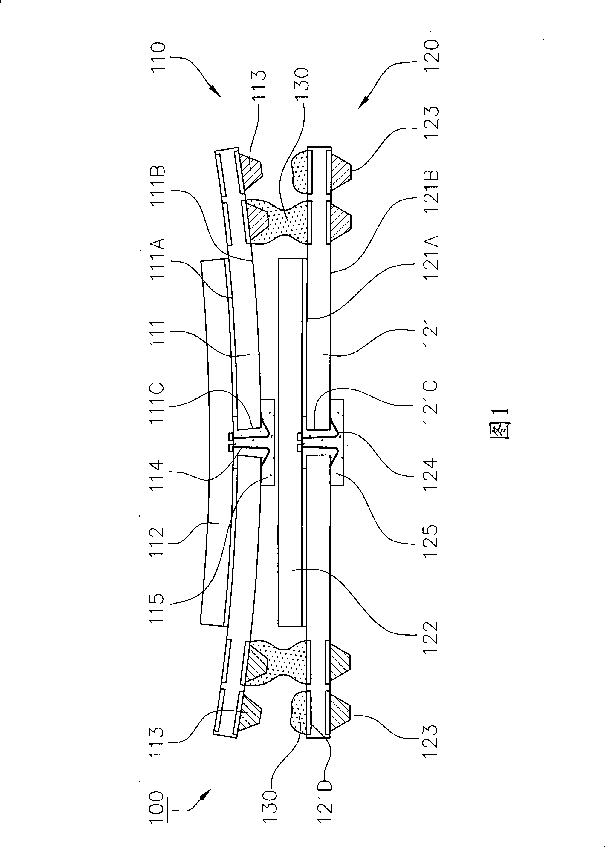
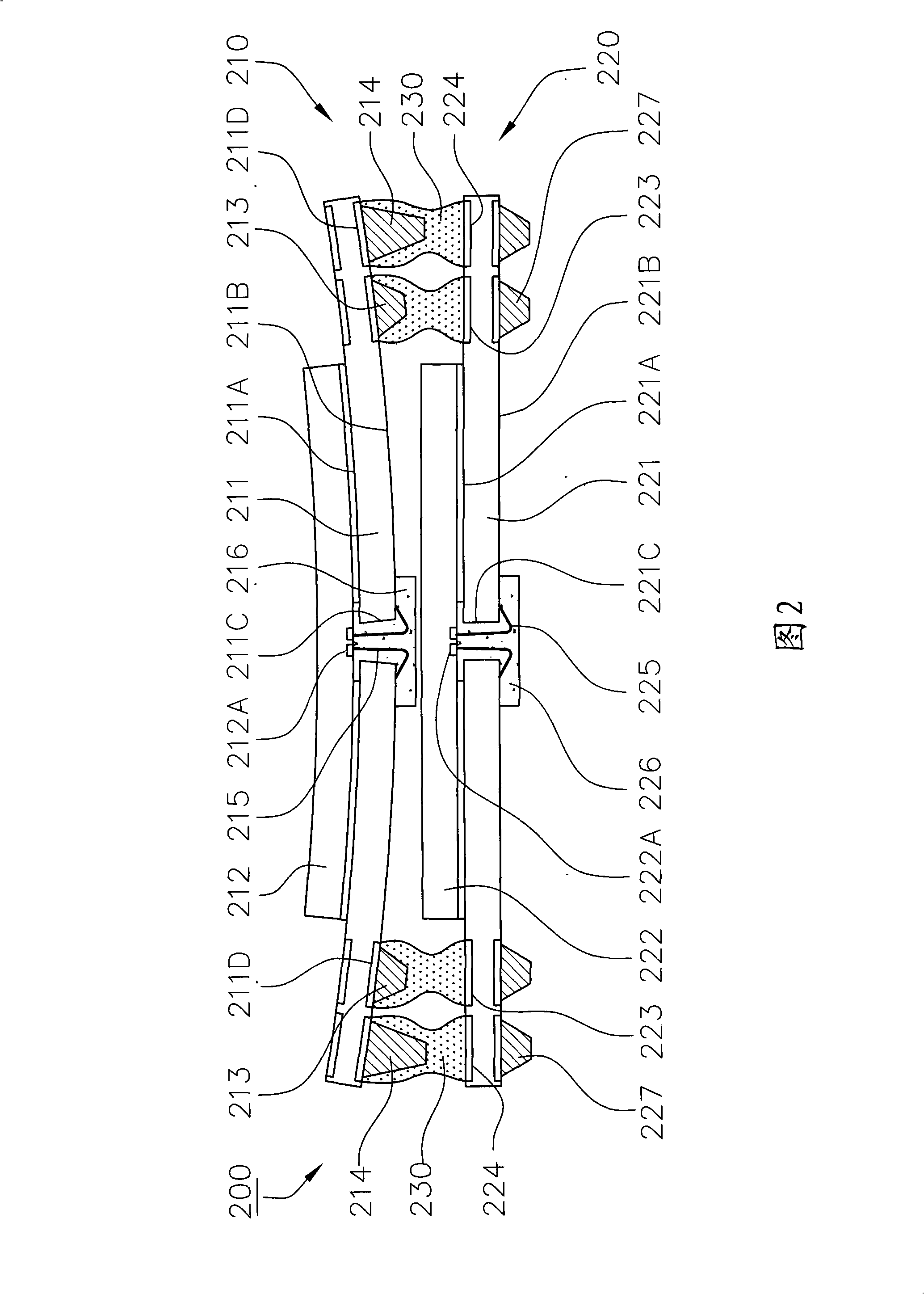
[0099] According to a first embodiment of the present invention, a semiconductor package bonding structure for avoiding soldering defects caused by substrate warpage is disclosed.

[0100] Please refer to FIG. 2 , which is a schematic cross-sectional view of a semiconductor package bonding structure according to a first embodiment of the present invention. A semiconductor package bonding structure 200 according to the first embodiment of the present invention mainly includes at least a first semiconductor package 210 , a package carrier 220 and a plurality of solders 230 . The first semiconductor package 210 is disposed on the package carrier 220 and connected and electrically connected to the package carrier 220 by the solders 230 .

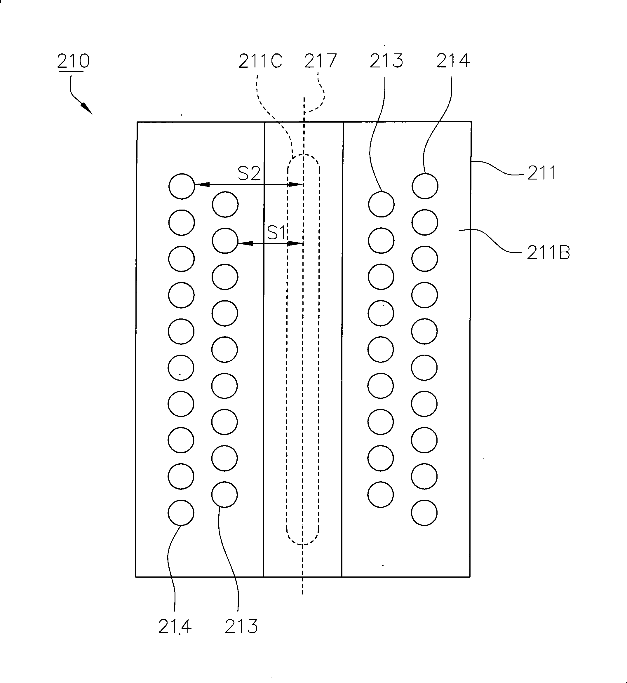
[0101] The aforementioned first semiconductor package 210 includes a first substrate 211 , a first chip 212 , a plurality of first external terminals 213 and a plurality of second external terminals 214 .

[0102] The first substrate 211 is use...

no. 3 Embodiment

[0116]Please refer to FIG. 5 , which is a schematic cross-sectional view of a semiconductor package bonding structure according to a third embodiment of the present invention. A semiconductor package bonding structure according to the third embodiment of the present invention mainly includes at least one semiconductor package 210, a package carrier 320 and a plurality of solders 330, wherein the semiconductor package 210 is the same as the first embodiment of the first embodiment. The semiconductor packages 210 are substantially the same, so they are labeled with the same reference numerals.

[0117] The aforementioned semiconductor package 210 includes a substrate 211, a chip 212, a plurality of first external terminals 213 and a plurality of second external terminals 214; wherein:

[0118] The first external terminals 213 and the second external terminals 214 are disposed on the lower surface 211B of the substrate 211 . Moreover, the distance from the first external termina...


PUM


Abstract

The invention relates to a semiconductor packaging and jointing structure, in particular to a semiconductor packaging and jointing structure for preventing welding defects caused by substrate warping, which mainly comprises at least a semiconductor packaging component, a package carrier and a solder. The solder is used for welding external terminals of the semiconductor packaging component to the package carrier. The external terminals of the semiconductor packaging component are at least divided into two groups according to different distances from the substrate centerline. In one embodiment, the external terminals of different groups contain bumps with different heights, the bumps are used for compensating solder clearance difference between connection end points of the external terminals and the package carrier caused by a preset warpage of the substrate, and the welding defects can not occur under the situation that the warpage of the substrate is predictable. In another embodiment, a compensation bump can be arranged between larger solder clearances. The semiconductor packaging and jointing structure can shorten the solder clearance difference caused under a predictable warpage of the substrate, can prevent the welding defects caused by substrate warping; and can integrate the functions of heat radiation and micro distance maintenance.

Description

technical field [0001] The present invention relates to a semiconductor package assembly and bonding technology, in particular to a semiconductor package bonding structure that avoids soldering defects caused by substrate warpage, and can be applied to a high-density 3D stacking structure (Package-On-Package module, POP ). Background technique [0002] With the current development trend of thinning semiconductor packages, the substrate of the semiconductor package becomes more likely to warp during the surface bonding reflow process, resulting in soldering defects such as cold soldering, empty soldering or false soldering. Especially in a package-on-package device (POP) of stacked semiconductor packages, soldering defects are a major problem in the bonding process. In order to meet the needs of advanced miniaturized electronic products, multiple semiconductor packages can be stacked vertically in 3D to meet the requirements of small surface bonding area and high-density com...

Claims


Application Information

Patent Timeline
IPC IPC(8): H01L25/00H01L25/065H01L23/488
CPCH01L2924/15311H01L2924/15331H01L2224/4824H01L2924/3511H01L2224/73215H01L2224/32225
Inventor 范文正
Owner POWERTECH TECHNOLOGY
Why Eureka
Try Eureka