Display
A display and light-emitting element technology, applied in the display field, can solve problems such as uneven lines, uneven spots, and disturbed deposition surfaces
- Summary
- Abstract
- Description
- Claims
- Application Information
AI Technical Summary
Problems solved by technology
Method used
Image

Examples
no. 1 example
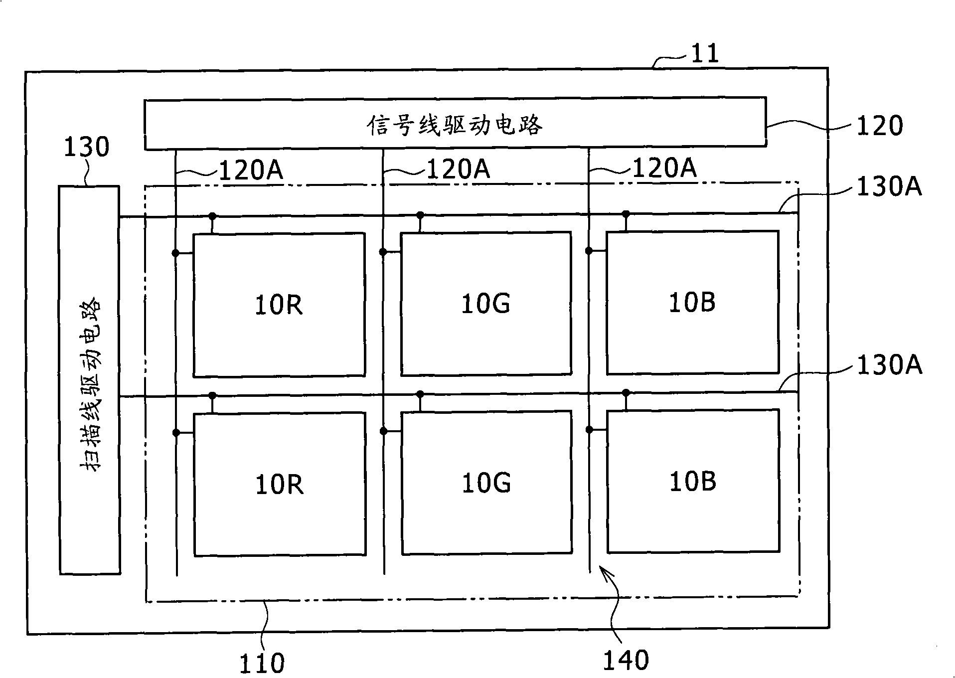
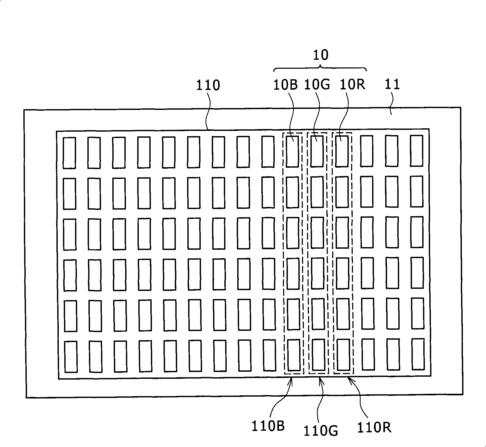
[0044] figure 1 A display structure according to a first embodiment of the present invention is shown. The display is used as an ultra-thin organic light-emitting color display and the like. For this display, for example, a display region 110 in which a plurality of organic light emitting elements 10R, 10G, and 10B described later are arranged in a matrix is formed on a receptor substrate 11 made of glass. Furthermore, around this display area 110, a signal line driver circuit 120 and a scan line driver circuit 130 are formed as drivers for video display.
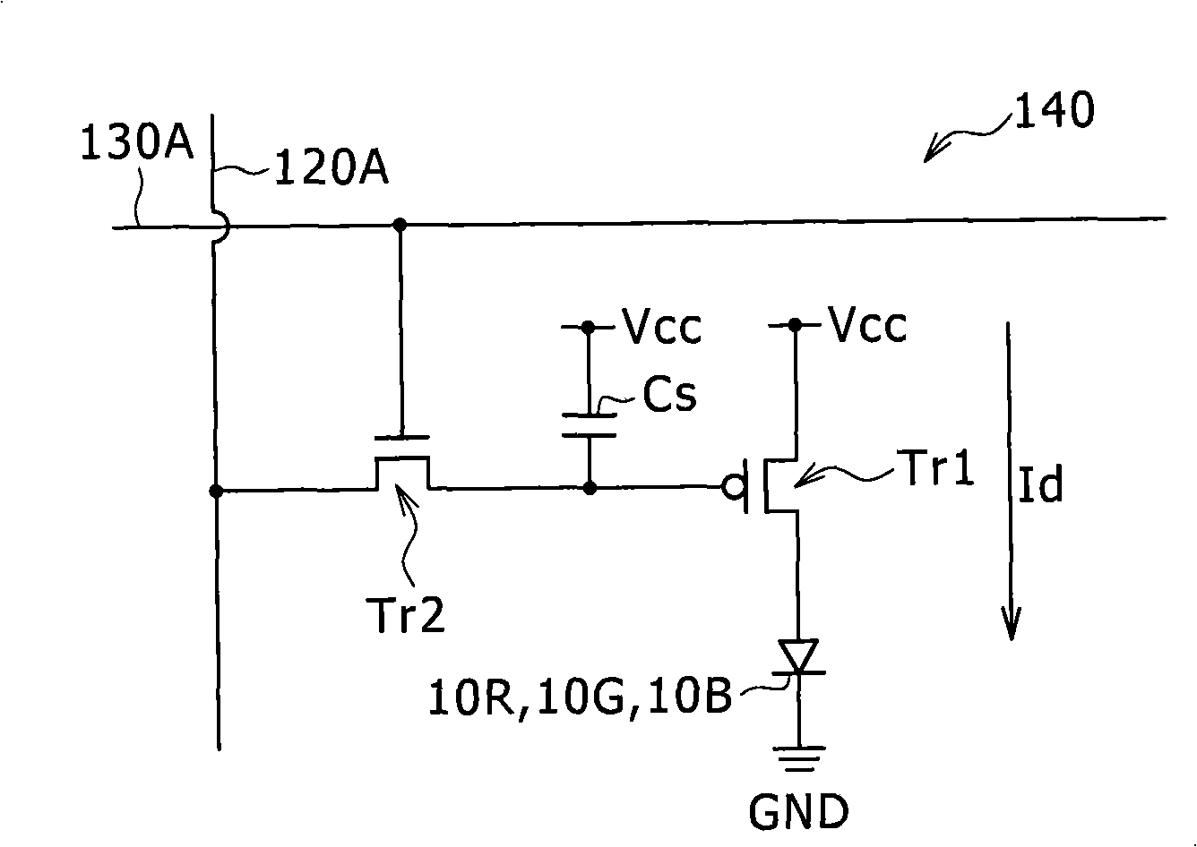
[0045] The pixel driving circuit 140 is formed in the display area 110 . figure 2One example of a pixel drive circuit 140 is shown. This pixel driving circuit 140 is formed under a first electrode described later, and is composed of a driving transistor Tr1, a writing transistor Tr2, a capacitor (holding capacitor) Cs between these transistors, and a first power supply line (Vcc) and An active driving circuit of the ...
no. 2 example
[0088] 18A and 18B show the shape of the insulating layer 14 in the display according to the second embodiment of the present invention. In this display, only the light emitting layer 15C of the organic light emitting elements 10R and 10G is the transfer light emitting layer 15C formed by transfer, while the organic light emitting element 10B is formed by a method other than transfer (for example, vapor deposition). Light emitting layer 15C. Furthermore, if the insulating layer 14 is equally distributed to each of the red, green, and blue light-emitting element columns 110R, 110G, and 110B, the contact area between the insulating layer 14 and the donor substrate 40 in the blue light-emitting element column 10B (i.e. , the area of the top surface of the relief 14A) is the largest. Due to this feature, its own reverse printing can be suppressed in the display. Therefore, occurrence of line unevenness and spot unevenness can be avoided, thereby improving display quality. In ...
example 1
[0094] Similar to the first embodiment, a display including the red and blue organic light emitting elements 10R and 10B was manufactured. During this manufacturing process, the width of the light emitting region 13A and the distances CC and DD were measured. As a result, the width of the light emitting region 13A was 70 μm, and the distances CC and DD were 78 μm and 122 μm, respectively. For each of the organic light emitting elements 10R and 10B, a light emitting layer 15C is formed by transfer. Changing the length of the longitudinal axis of the beam spot of the laser light to a different value in the range of 70 to 130 μm results in changing the width W of the light emitting layer 15C in the row direction to a different value in the range of 70 to 130 μm. The minor axis of the beam spot of the laser was fixed at 20 μm, and the laser was moved to scan in a direction perpendicular to the longitudinal direction of the laser beam spot. Set the wavelength and energy density o...
PUM
 Abstract
Description
Claims
Application Information
 - R&D
- Intellectual Property
- Life Sciences
- Materials
- Tech Scout
- Unparalleled Data Quality
- Higher Quality Content
- 60% Fewer Hallucinations
Browse by: Latest US Patents, China's latest patents, Technical Efficacy Thesaurus, Application Domain, Technology Topic, Popular Technical Reports.
© 2025 PatSnap. All rights reserved.Legal|Privacy policy|Modern Slavery Act Transparency Statement|Sitemap|About US| Contact US: help@patsnap.com