LCD panel and its sealing method

A liquid crystal display panel and substrate technology, applied in nonlinear optics, instruments, optics, etc., can solve the problems of inconvenience, general products and methods without suitable structures and methods, etc., to reduce packaging costs, simplify the sealing process, and improve efficiency effect

Inactive Publication Date: 2009-01-14
AU OPTRONICS (SUZHOU) CORP LTD +1
View PDF0 Cites 10 Cited by
  • Summary
  • Abstract
  • Description
  • Claims
  • Application Information

AI Technical Summary

Problems solved by technology

[0006] It can be seen that the above-mentioned existing liquid crystal display panel and its sealing method obviously still have inconvenience and defects in product structure, manufacturing method and use, and need to be further improved urgently.
In order to solve the above-mentioned problems, the relevant m

Method used


Image

  • LCD panel and its sealing method
  • LCD panel and its sealing method
  • LCD panel and its sealing method

Examples


Embodiment Construction

[0041] In order to further explain the technical means and effects of the present invention to achieve the intended purpose of the invention, in conjunction with the accompanying drawings and preferred embodiments, the specific implementation, structure, method, The steps, features and effects are described in detail below.

[0042] The foregoing and other technical contents, features and effects of the present invention will be clearly presented in the following detailed description of the preferred embodiment with reference to the drawings. Through the description of the specific embodiments, it is possible to gain a more in-depth and specific understanding of the technical means and effects adopted by the present invention to achieve the predetermined purpose. However, the accompanying drawings are only for reference and explanation purposes, and are not used for the present invention. Be restricted.

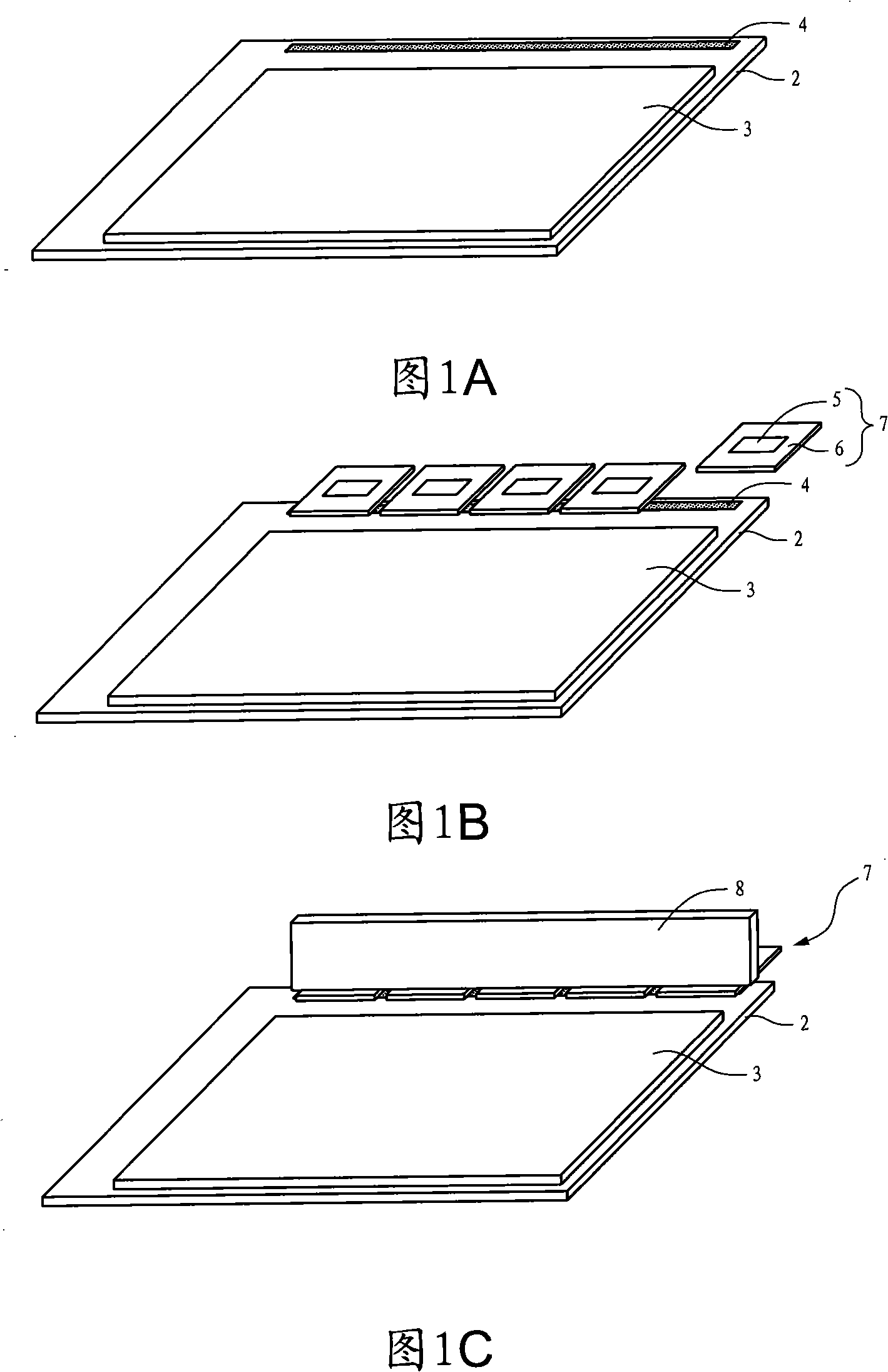
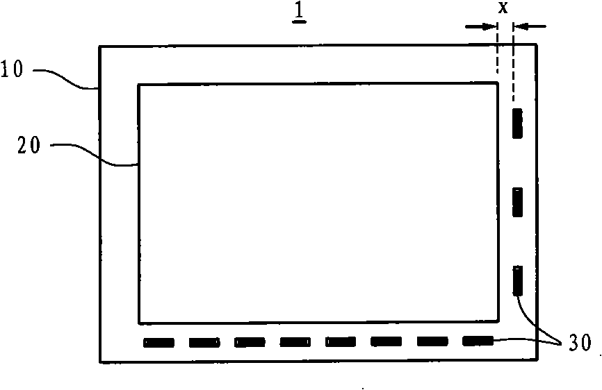
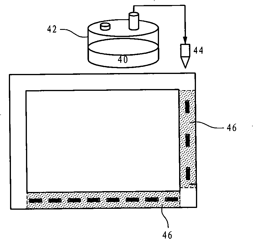
[0043] See Figure 2A-2C , Which illustrates a schematic diagram of a method...


PUM


Abstract

The invention relates to an LCD panel and a corresponding sealing method. The LCD panel is provided with a first base plate and a second base plate; wherein, the first base plate is provided with a plurality of connecting cushions and the second base plate is arranged on the same surface with the connecting cushions. Then a semi-flow anisotropic conductive film is painted onto the connecting cushions and then a chip unit is pressed in a hot manner onto the anisotropic conductive film to lead the chip unit to be electrically connected with the connecting cushions through the anisotropic conductive film and also to lead the anisotropic conductive film to be cured so as to seal a clearance between the second base plate and the connecting cushions. The semi-flow anisotropic conductive film provided by the invention can simultaneously complete the sealing and communicating functions, thus simplifying the assembling process of the LCD panel and reducing the sealing cost.

Description

Technical field [0001] The invention relates to a liquid crystal display panel and a sealing method thereof, in particular to a liquid crystal display panel using a semi-fluid anisotropic conductive adhesive and a sealing method thereof. Background technique [0002] The composition of Anisotropic Conductive Film (ACF) includes conductive particles and insulating materials. ACF is a polymer material with both unidirectional conductivity and glue fixation. Currently, it is mostly used in Chip On Glass (COG), Tape Carrier Package / Chip On Film (TCP). / COF), chip (ie chip, hereinafter referred to as chip) direct packaging (Chip On Board, COB) and flexible printed circuit (FPC) manufacturing process. Among them, driver IC-related package bonding is the most popular Attention. [0003] Please refer to FIGS. 1A-1C, which illustrate the ACF attaching process in the prior art. Please refer to FIG. 1A, the liquid crystal panel (Cell) has a first substrate 2 and a second substrate 3. First,...

Claims


Application Information

Patent Timeline
IPC IPC(8): G02F1/13
Inventor 陈晋
Owner AU OPTRONICS (SUZHOU) CORP LTD
Why Eureka
Try Eureka