High voltage metal-oxide-semiconductor transistor and manufacturing method thereof

A technology of oxide semiconductors and manufacturing methods, which is applied in the direction of semiconductor/solid-state device manufacturing, semiconductor devices, electrical components, etc., can solve the problems of unfavorable integrated circuit component size reduction and integration improvement, increase component area, etc., and reduce the surface area. Effects of electric field, increased current path, and improved breakdown voltage

Inactive Publication Date: 2009-01-14
UNITED MICROELECTRONICS CORP
View PDF0 Cites 6 Cited by
  • Summary
  • Abstract
  • Description
  • Claims
  • Application Information

AI Technical Summary

Problems solved by technology

Although the formation of isolation structures in high-voltage components can increase the breakdown voltage, this method will increase the area of ​​the components, which is not conducive to the trend of reducing the size of integrated circuit components and increasing the integration level.

Method used


Image

  • High voltage metal-oxide-semiconductor transistor and manufacturing method thereof
  • High voltage metal-oxide-semiconductor transistor and manufacturing method thereof
  • High voltage metal-oxide-semiconductor transistor and manufacturing method thereof

Examples


Embodiment Construction

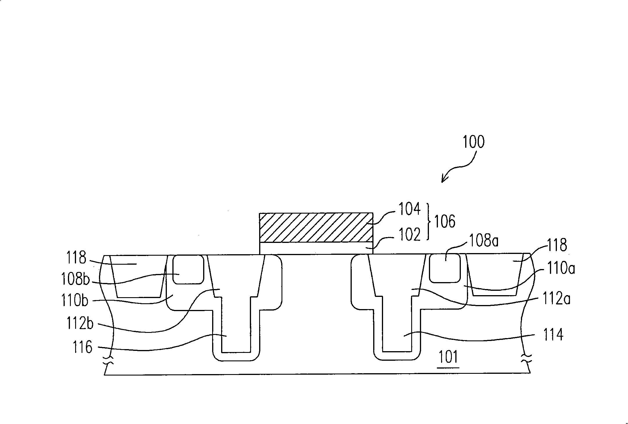
[0047] figure 1 It is a schematic cross-sectional view of a high-voltage metal-oxide-semiconductor transistor according to an embodiment of the present invention.

[0048] Please refer to figure 1 , the high-voltage metal oxide semiconductor transistor 100 of this embodiment includes a first-type doped substrate 101, a gate structure 106, a second-type drain region 108a, a second-type source region 108b, and second-type drift regions 110a and 110b , the first isolation structures 112 a and 112 b and the second isolation structures 114 and 116 .

[0049] The first-type doped substrate 101 is, for example, a well region or an epitaxial layer, and the first-type doped substrate 101 has two element isolation structures 118 . The first isolation structures 112a and 112b are respectively disposed in the first-type doped substrate 101 . The first isolation structures 112a and 112b are, for example, shallow trench isolation (STI). The material of the first isolation structures 112...


PUM


Abstract

The invention provides a high-voltage metal oxide semiconductor transistor, comprising a doped substrate, two first separation structures, a grid structure, a source area, a drain area, two separation structures and two shifting areas; wherein, two first separation structures are respectively arranged in the doped substrate; the grid structure is arranged on part of the two first separation structures and the doped substrate between the two first separation structures; the source area and the drain area are respectively arranged in the doped substrate at one side of the two first separation structures; two second separation structures are respectively arranged below the two first separation structures; furthermore, the upper surface of the second separation structure is less than the lower surface of the first separation structure; two shifting areas are respectively arranged in the doped substrate; furthermore, the source area, the drain area, two first separation structures and two second separation structures are surrounded.

Description

technical field [0001] The present invention relates to an integrated circuit device and a manufacturing method thereof, and more particularly, to a high voltage metal oxide semiconductor transistor and a manufacturing method thereof. Background technique [0002] Among integrated circuit components, different circuits require close cooperation of different circuit components with different underlying operating characteristics. Among them, the high-voltage component, as the name suggests, is a component that can withstand higher bias voltage, which means that the breakdown voltage of the high-voltage component is higher than that of the general component. [0003] The conventional high-voltage device is mainly formed by using an isolation structure to increase the junction breakdown voltage of the source / drain regions, so that the high-voltage device can still operate normally under the condition of high voltage. Although the formation of the isolation structure in the high...

Claims


Application Information

Patent Timeline
IPC IPC(8): H01L29/78H01L21/336
CPCH01L29/7833H01L29/0847H01L29/0653
Inventor 吴荣宗陈冠全戴炘吕安泰张堡安
Owner UNITED MICROELECTRONICS CORP
Why Eureka
Try Eureka