LED device and its preparing process

A technology for light-emitting diodes and manufacturing methods, which is applied in semiconductor/solid-state device manufacturing, electrical components, circuits, etc., can solve the problems of increasing metal particles, adhesion, etc., and achieve the effect of avoiding leakage current increase, saving cutting cost and yield.

Active Publication Date: 2009-01-14
DELTA ELECTRONICS INC
View PDF0 Cites 8 Cited by
  • Summary
  • Abstract
  • Description
  • Claims
  • Application Information

AI Technical Summary

Problems solved by technology

Therefore, in addition to the need for a cutting process, the probability of metal particles adhering to the sidewall of the laminate is also increased.

Method used


Image

  • LED device and its preparing process
  • LED device and its preparing process
  • LED device and its preparing process

Examples


Embodiment Construction

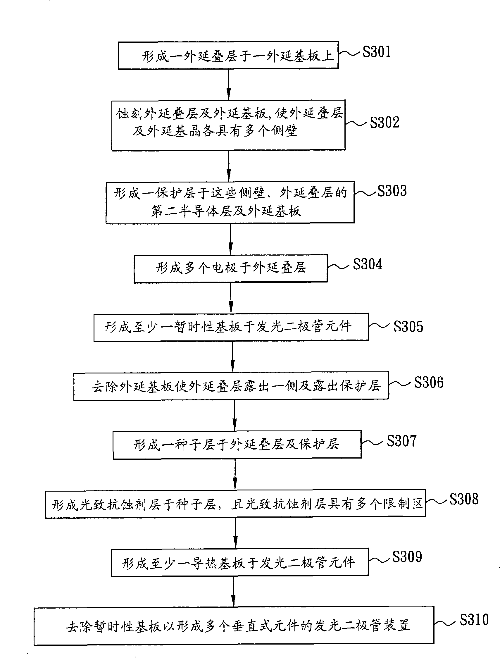
[0048] A method of manufacturing a light emitting diode device according to a preferred embodiment of the present invention will be described below with reference to related drawings.

[0049] Please refer to image 3 , a method for manufacturing a light emitting diode device 4 according to a preferred embodiment of the present invention, which includes steps S301 to S310. Please also refer to the following Figure 4A to Figure 4H shown.

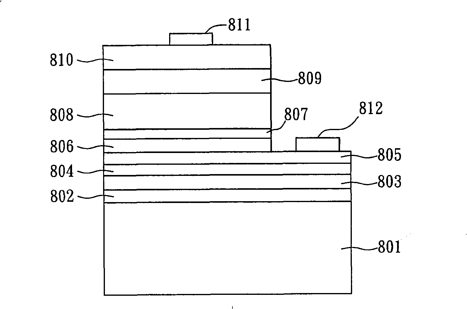
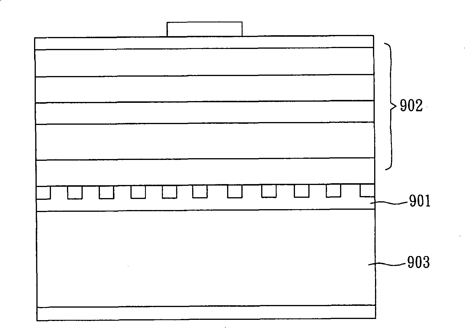
[0050] Such as Figure 4A As shown, step S301 forms an epitaxial stack E on the epitaxial substrate 403 . Wherein, the epitaxial stack E includes a first semiconductor layer 404 , a light emitting layer 405 and a second semiconductor layer 406 . The first semiconductor layer 404 is formed on the epitaxial substrate 403 , then the light emitting layer 405 is formed on the first semiconductor layer 404 , and then the second semiconductor layer 406 is formed on the light emitting layer 405 .

[0051] In the above embodiment, the first semi...


PUM


Abstract

The invention discloses an LED device and a preparation method thereof; the LED device comprises an external extension lamination layer, a heat conduction substrate and a seed layer. The external extension lamination layer is sequentially provided with a first semiconductor layer, a luminescent layer and a second semiconductor layer; the heat conduction substrate and the fist semiconductor layer are arranged correspondingly to each other; the seed layer is arranged between the first semiconductor layer and the heat conduction substrate; wherein, the first semiconductor is an N-typed external extension layer; furthermore, the second semiconductor layer is a P-typed external extension layer. The preparation method of the invention comprises the steps as follows: a temporary substrate is formed on the LED element; at least one heat conduction substrate is formed on the LED element. The material of the temporary substrate comprises a solidified polymer material.

Description

technical field [0001] The invention relates to a light emitting diode device and a manufacturing method thereof. Background technique [0002] A light emitting diode (light emitting diode, LED) device is a light emitting element made of semiconductor material. Since the light-emitting diode device is a cold light emitting device, it has the advantages of low power consumption, long component life, fast response speed, etc., coupled with the characteristics of small size and easy to make extremely small or array components, so in recent years with the continuous advancement of technology , and its application range covers indicator lights of computers or home appliances, backlights of liquid crystal display devices, traffic signals or vehicle lights. [0003] In order to increase the luminous efficiency of the LED device, in the known technology, a metal reflective substrate is disposed on the LED element, thereby reflecting light to improve the luminous efficiency. Howeve...

Claims


Application Information

Patent Timeline
Patent Type & Authority Applications(China)
IPC IPC(8): H01L33/00H01L21/782H01L33/02H01L33/64
Inventor 薛清全陈世鹏陈朝旻陈煌坤
Owner DELTA ELECTRONICS INC
Why Eureka
Try Eureka