
Drive circuit and inverter for voltage driving type semiconductor device

A technology of voltage drive and drive circuit, which is applied in the direction of electrical components, output power conversion devices, and conversion equipment without intermediate conversion to AC, which can solve the problem of increased conduction resistance, increase of conduction loss, and the cost of inverter drive circuits. Problems such as increase in size and size, to achieve the effect of preventing loss and increasing costs

Inactive Publication Date: 2009-01-14
HITACHI LTD
View PDF2 Cites 33 Cited by
  • Summary
  • Abstract
  • Description
  • Claims
  • Application Information

AI Technical Summary

Problems solved by technology

However, using a negative voltage power supply has a problem of increasing the cost and size of the inverter drive circuit
[0013] On the other hand, a method of applying a negative voltage to the gate during turn-off without using a negative voltage power supply has been proposed (for example, Patent Document 2). The power supply voltage is low, so there is a problem that the on-resistance increases and the conduction loss increases

Method used


Image

  • Drive circuit and inverter for voltage driving type semiconductor device
  • Drive circuit and inverter for voltage driving type semiconductor device
  • Drive circuit and inverter for voltage driving type semiconductor device

Examples


Embodiment Construction

[0060] Hereinafter, embodiments of the present invention will be described with reference to the drawings.

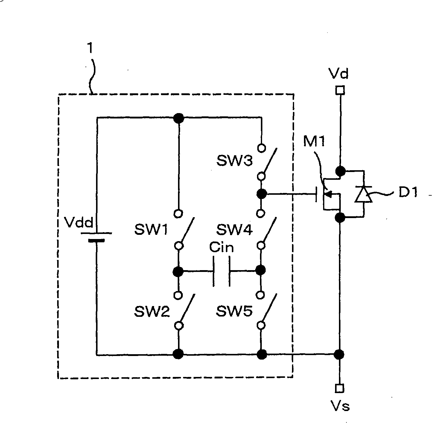
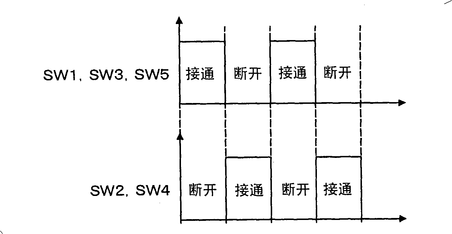
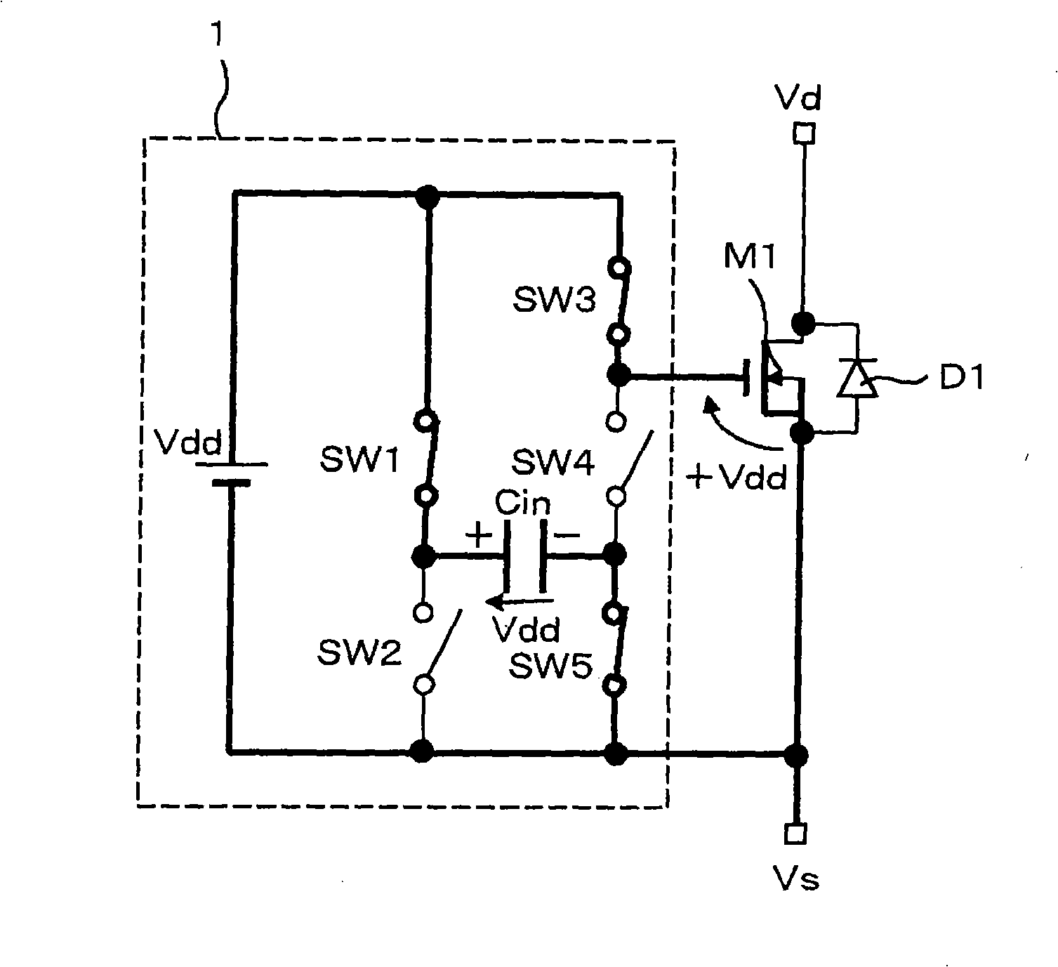
[0061] figure 1 It is a diagram showing the first embodiment of the present invention, and shows a diagram describing an example of a power MOSFET (M1) as a voltage-driven semiconductor element. It consists of a diode D1 built into the power MOSFET (M1), a drive circuit 1 for the power MOSFET (M1), a DC power supply voltage Vdd, five switches (SW1 to SW5), and a capacitor Cin. The first switch SW1 is connected to the positive side of the DC power supply voltage Vdd, the second switch SW2 is connected to the other terminal of the first switch SW1 and the negative side of the DC power supply voltage Vdd, and the third switch SW3 is connected to the DC power supply voltage Vdd. The positive side of the fourth switch SW4 is connected to the other terminal of the third switch SW3 and the fifth switch SW5, and the fifth switch SW5 is connected to the other terminal of the f...


PUM


Abstract

The invention provides a drive circuit for voltage driving type semiconductor device capable of solving the problem that the grid is required being negative potential state and the negative voltage power is required in the drive circuit when the semiconductor device is turn off, in order to prevent erroneously being ignited. The drive circuit for driving a semiconductor element is equipped with: a first switch connected to a positive side of a DC power supply; a second switch connected to the other terminal of the first switch and to a negative side of the DC power supply; a third switch connected to the positive side of the DC power supply; a fourth switch connected to the other terminal of the third switch; a fifth switch connected to the other terminal of the fourth switch and to the negative side of the DC power supply; and a capacitor connected to the other terminal of the first switch and to the other terminal of the fourth switch. In the drive circuit, a gate of the semiconductor element is connected to the other terminal of said third switch; and a source of the semiconductor element is connected to the negative side of the DC power supply. Therefore the negative voltage is applied on the grid of the semiconductor device only using the source supply of position voltage.

Description

technical field [0001] The present invention relates to a drive circuit and an inverter device for a voltage-driven semiconductor element used in a power converter. Background technique [0002] Compared with current-driven semiconductor devices such as thyristors, voltage-driven semiconductor devices such as power MOSFETs (Metal Oxide Semiconductor Field Effect Transistor) and IGBTs (Insulated Gate Bipolar Transistor) have many advantages such as small drive circuits and low loss. . Figure 10 This is a configuration diagram of a single-phase inverter using power MOSFETs as voltage-driven semiconductor elements. [0003] exist Figure 10 In the configuration diagram of FIG. 1 , power MOSFETs (M1-M4), diodes (D1-D4) mounted inside the power MOSFETs, a power supply voltage Vin, and an inductor 14 as a load are provided. Connect the drive circuits G1 to G4 to the power MOSFETs. The details of the drive circuits G1 to G4 are in Figure 11 Indicated. [0004] The driving circ...

Claims


Application Information

Patent Timeline
Patent Type & Authority Applications(China)
IPC IPC(8): H02M1/08H02M7/537H02M7/5387
CPCH02M7/5387H02M2003/071H02M7/48H02M1/08H02M3/07H02M3/071H03K17/00
Inventor 桥本贵之平尾高志白石正树
Owner HITACHI LTD
Learn More