Multi-chip encapsulation construction of large power

A multi-chip packaging and high-power technology, which is applied in the direction of electrical components, electrical solid devices, circuits, etc., can solve problems such as failure, inability to dissipate heat in a timely manner, and large chip current heating, achieving high heat dissipation efficiency, simple packaging and processing technology, Effect of improving reliability and yield

Active Publication Date: 2009-02-04
浙江华越芯装电子股份有限公司
View PDF0 Cites 3 Cited by
  • Summary
  • Abstract
  • Description
  • Claims
  • Application Information

AI Technical Summary

Problems solved by technology

Often due to the high-power device working chip current heating is too large, unable to dissipate heat in time, resulting in failure

Method used


Image

  • Multi-chip encapsulation construction of large power
  • Multi-chip encapsulation construction of large power

Examples


Embodiment Construction

[0027] In order to have a further understanding of the purpose, structure, features and functions of the present invention, the detailed description is as follows in conjunction with the embodiments.

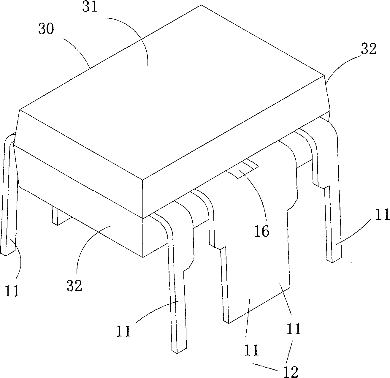
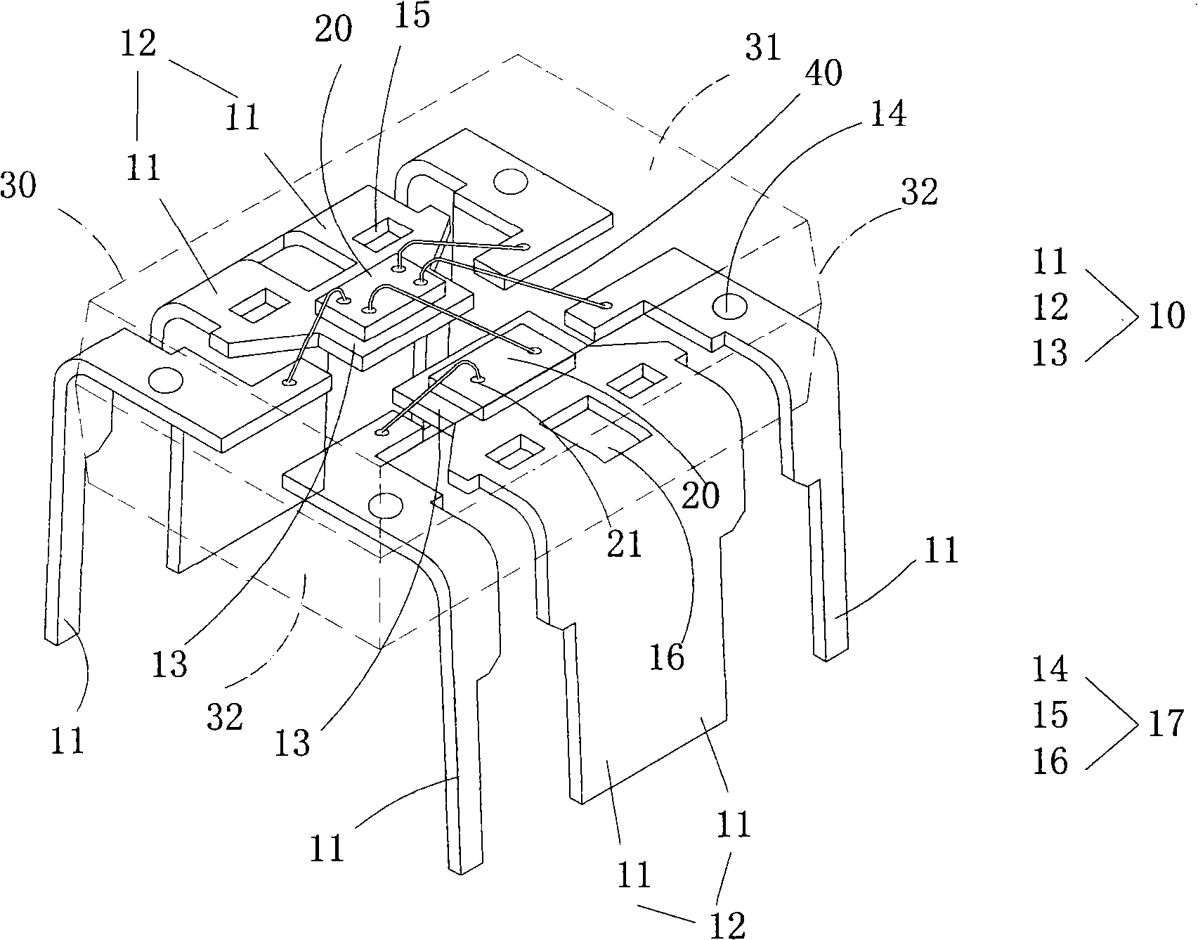
[0028] In order to enable them to be mixed and packaged together without affecting the function definition and geometric shape of standard integrated circuit chips, and comply with current industry specifications for chip packaging, the present invention provides a high-power multi-chip packaging structure. It has a plurality of bearing boards, and each bearing board has pins connected to dissipate heat, which can improve the heat dissipation efficiency of the integrated circuit, improve product reliability, reduce manufacturing cost, and improve product yield.

[0029] Such as figure 1 , figure 2 As shown, it is a schematic diagram of a high-power multi-chip packaging structure according to a preferred embodiment of the present invention, including a lead frame 10, two differ...


PUM


Abstract

The invention discloses an enclosure for multiple large-power chips, belonging to semiconductor enclosure technical field. The enclosure comprises a lead frame which is provided with a plurality of pins at both sides; each side of the center of the lead frame is provided with at least one chip carrier plate and each chip carrier plate is respectively connected to the two corresponding pins on the same side; the two pins connected with the same chip carrier plate are connected, forming heat dissipating pins; and locating holes are arranged on both the pins and the heat dissipating pins. The invention mixes and encloses a plurality of chips of a large-power device, so heat dissipation efficiency is high and encapsulation process is simple, which is good for improving the reliability and yield of the product.

Description

technical field [0001] The invention discloses a high-power multi-chip package structure, which belongs to the technical field of semiconductor package structures. Background technique [0002] With the further improvement of integrated circuit miniaturization and integration, multi-chip packaging structures have appeared more and more, but generally they are stacked or system integrated on a small PCB. Higher requirements lead to yield and cost problems, especially for high-power integrated circuit products with strong heat dissipation requirements. Often because the current of the high-power device working chip heats up too much, it cannot dissipate heat in time, resulting in failure. This is also a difficulty in the miniaturized multi-chip hybrid packaging of high-power devices. Contents of the invention [0003] The invention provides a high-power multi-chip packaging structure that can meet the requirements of electrothermal characteristics (high current and good he...

Claims


Application Information

Patent Timeline
Patent Type & Authority Applications(China)
IPC IPC(8): H01L25/00H01L25/065H01L25/18H01L23/488H01L23/495H01L23/367H01L23/31
CPCH01L2224/48137H01L2224/48247H01L2924/181H01L2924/00012
Inventor 张永夫林刚强
Owner 浙江华越芯装电子股份有限公司
Why Eureka
Try Eureka