Manufacturing method of hollowed-out PCB
一种制作方法、电路板的技术,应用在印刷电路制造、印刷电路、印刷电路等方向,能够解决线路侧蚀、高度差、过蚀等问题
- Summary
- Abstract
- Description
- Claims
- Application Information
AI Technical Summary
Problems solved by technology
Method used
Image
Examples
Embodiment Construction
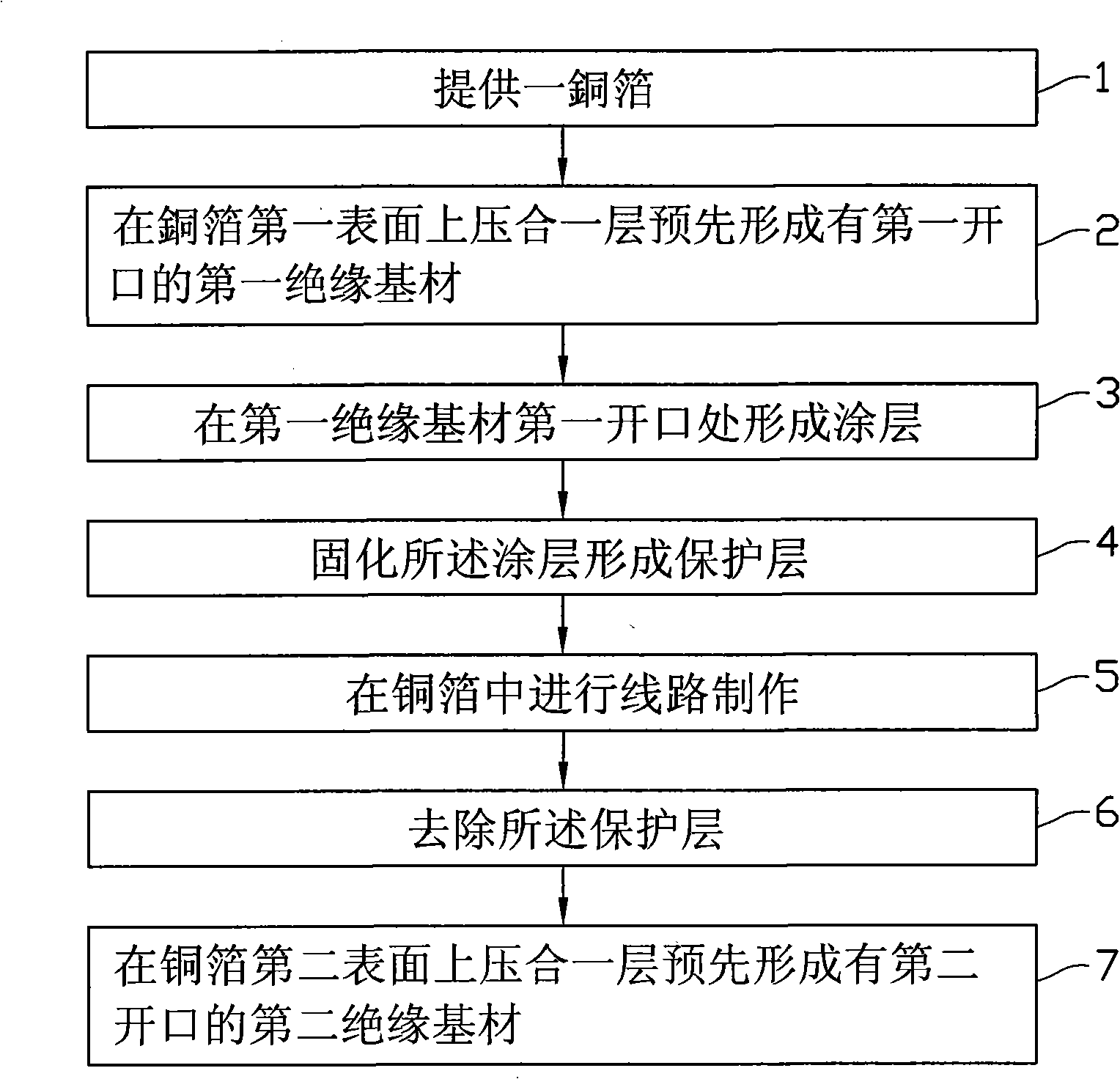
[0017] refer to figure 1 , the hollow circuit board manufacturing method provided by the technical solution includes the following steps:
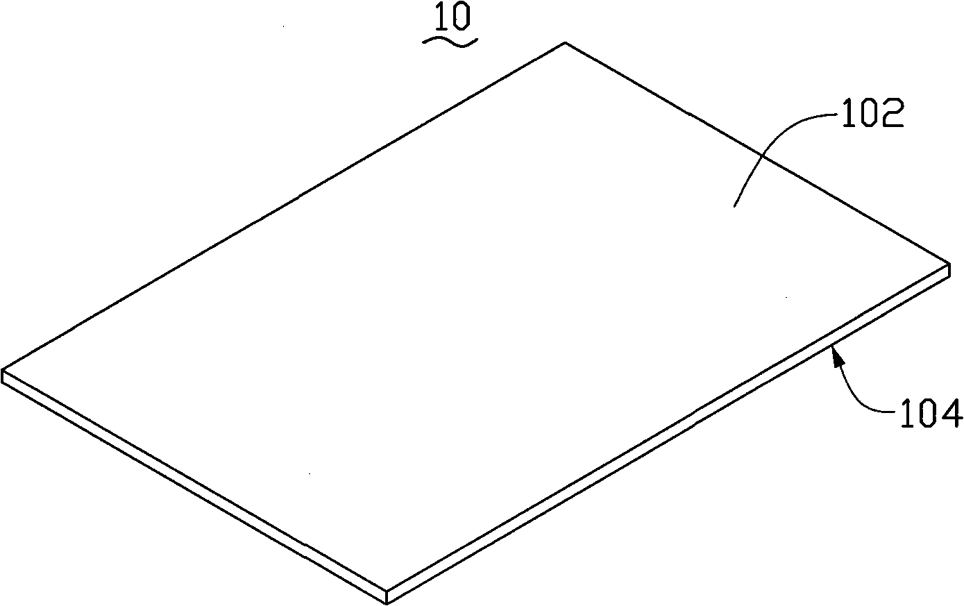
[0018] Step 1, see figure 2 , providing a copper foil 10 . Copper foil 10 may be electrolytic copper foil or rolled copper foil. The copper foil 10 includes a first surface 102 and a second surface 104 opposite to each other. Preferably, the copper foil 10 may be treated with an acid cleaning solution to remove dirt on the first surface 102 and the second surface 104 of the copper foil and increase the roughness of the first surface 102 and the second surface 104 of the copper foil.
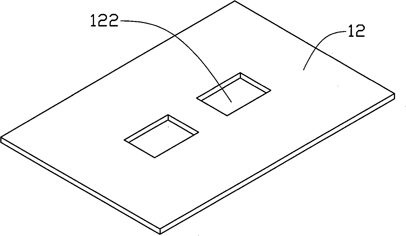
[0019] Step 2, pressing the first insulating substrate 12 preformed with the first opening 122 on the first surface 102 of the copper foil 10 .
[0020] refer to image 3 , there are two first openings 122 on the first insulating substrate 12 . Of course, one or more first openings can also be provided on the first insulating substrate 12 according to ...
PUM
| Property | Measurement | Unit |
|---|---|---|
| hardness | aaaaa | aaaaa |
Abstract
Description
Claims
Application Information


