Process for manufacturing graph in circuit burying mode

A pattern and line technology, which is applied in the field of pattern making process, can solve the problems of line side etching and uneven bottom edge of the line, and achieve the effect of avoiding the side etching problem, smooth line edge and uniform line width.

Active Publication Date: 2021-01-01
GUANGZHOU TERMBRAY ELECTRONICS TECH CO LTD
View PDF14 Cites 0 Cited by
  • Summary
  • Abstract
  • Description
  • Claims
  • Application Information

AI Technical Summary

Problems solved by technology

It solves the problem that the traditional PCB graphic manufacturing process adopts the process of "making graphic protective layer-etching-removing protective layer" to make lines. During the etching process, the etching potion will attack the area to be etched and the side wall of the protected graphic at the same time, resulting in "side erosion" of the line. "phenomenon, the circuit completed in this way is not a "rectangular" shape but a "trapezoidal" shape, and the completed circuit often has the problem that the bottom edge of the circuit is uneven
This has a great adverse effect on the integrity of electrical signal transmission and the need to make more sophisticated circuits

Method used


Image

  • Process for manufacturing graph in circuit burying mode
  • Process for manufacturing graph in circuit burying mode

Examples


Embodiment 1

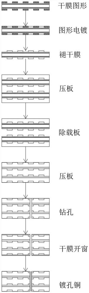
[0028] A process for making graphics in the form of buried lines, comprising the following steps:

[0029] S1. Making the carrier core board: Paste the copper layer on both sides of the carrier board with an adhesive. The adhesive used in S1 is epoxy adhesive or acrylic acid adhesive. Use the carrier core board to replace the conventional core board , the carrier core board is composed of a carrier board, an adhesive layer and a copper layer. After pressing the board, the strength of the adhesive layer will decrease, and the copper layer and the carrier layer can be directly separated;

[0030] S2. Make dry film graphics: attach the dry film to both sides of the carrier core board, and make the graphics to be plated on the dry film, use the graphics electroplating method to make the required graphics on the carrier core board, and use the graphics electroplating method to make Graphics, there is no traditional etching process in the follow-up;

[0031] S3. Graphic electroplat...

Embodiment 2

[0042] A process for making graphics in the form of buried lines, comprising the following steps:

[0043] S1. Making the carrier core board: Paste the copper layer on both sides of the carrier board with an adhesive. The adhesive used in S1 is epoxy adhesive or acrylic adhesive;

[0044] S2. Make dry film graphics: attach the dry film to both sides of the carrier core board, and make graphics to be plated on the dry film;

[0045] S3. Graphic electroplating: electroplating the carrier core board after the dry film is attached, so that the exposed part of the carrier core board is plated with a copper layer;

[0046] S4, take off the dry film: take off the dry film on the carrier core plate after the copper layer is plated;

[0047] S5. Pressing plate: pressing multiple carrier core plates after copper plating;

[0048] S6. Remove the carrier board: separate the copper layer on the carrier core board from the carrier board, and remove the carrier board;

[0049] S7. Micro-e...

Embodiment 3

[0051] A process for making graphics in the form of buried lines, comprising the following steps:

[0052] S1. Making the carrier core board: Paste the copper layer on both sides of the carrier board with an adhesive. The adhesive used in S1 is epoxy adhesive or acrylic adhesive;

[0053] S2. Make dry film graphics: attach the dry film to both sides of the carrier core board, and make graphics to be plated on the dry film;

[0054] S3. Acid etching: Etch the copper layer not covered by the dry film with an acidic reagent, leaving the copper layer with the desired pattern;

[0055] S4. Film fading: remove the dry film on the surface of the core board after etching to complete the acid etching process.


PUM


Abstract

The invention discloses a process for manufacturing a graph in a circuit burying mode. The process comprises the following steps: pasting copper foils to the two sides of a carrier plate through an adhesive; attaching a dry film to the carrier copper foil, and manufacturing a to-be-plated pattern on the dry film; electroplating the carrier core plate to which the dry film is attached; taking downthe dry film on the carrier core plate plated with the copper layer; laminating the plurality of carrier core plates plated with the copper layers; separating the copper layer on the carrier core plate from the carrier plate; pressing the core plate after the carrier plate is taken out again; drilling a hole in the laminated core plate; cleaning and wetting the drilled hole; attaching dry films tothe surfaces of the two sides of the laminated core plate, and forming holes in the drilled positions of the core plate; carrying out metallization treatment on the holes in the dry film openings inthe core plate; and taking down the dry films on the surfaces of the two sides of the core plate. The method has the advantages that the etching side etching problem is avoided, the manufactured circuit better meets the design requirement, and the capacity of a factory for manufacturing a board with a finer circuit is improved under the condition that traditional PCB equipment conditions are not changed.

Description

technical field [0001] The invention relates to the technical field of PCB technology, in particular to a technology for making graphics by embedding lines. Background technique [0002] With the development of electronic technology, customers' requirements for PCB are becoming more and more stringent. Many new electronic products require PCB to be more precise and stable. However, traditional PCB graphics technology and manufacturing equipment have been difficult to meet new customer needs. The purpose of this new process is to produce more precise and stable circuit patterns without making major changes to the traditional PCB process and manufacturing equipment. [0003] The traditional PCB graphics manufacturing process adopts the process of "making graphic protection layer-etching-removing the protective layer" to make lines. During the etching process, the etching solution will attack the area to be etched and the side wall of the protected graphics at the same time, re...

Claims


Application Information

Patent Timeline
Patent Type & Authority Applications(China)
IPC IPC(8): H05K3/00H05K3/04H05K3/18
CPCH05K3/188H05K3/0047H05K3/04
Inventor 彭攀李德英
Owner GUANGZHOU TERMBRAY ELECTRONICS TECH CO LTD
Why Eureka
Try Eureka