
A semiconductor device and a method of manufacture thereof

一种半导体、器件的技术,应用在光电子半导体器件及其制造领域,能够解决不适于制备量子点有源区、器件加工复杂、器件复杂等问题

Inactive Publication Date: 2009-02-18
SHARP KK
View PDF13 Cites 3 Cited by
  • Summary
  • Abstract
  • Description
  • Claims
  • Application Information

AI Technical Summary

Problems solved by technology

Disadvantages of these vertical stacking methods include: vertically stacked devices with different emission wavelengths are complex and costly, device processing is very complex requiring independent control of currents introduced into devices with different emission wavelengths during operation, and it is necessary to separate grows each active region with an independent emission wavelength
The obvious disadvantage of these methods is that although only one substrate is used, for each individual emission wavelength, epitaxial growth of the entire device structure is required
A significant disadvantage of this selective area epitaxy method is that it relies on direct epitaxial growth onto the mask surface, and thus residual contamination induced at the surface during mask fabrication can degrade the properties of the final quantum dots
Another significant limitation of this method is that the mask is deposited on the substrate surface each time a new SK growth is performed, so this method is not suitable for preparing quantum dot active regions for light-emitting devices where, SK growth of more than one layer is often performed in each device structure so that the emission intensity from the light-emitting device can be high

Method used


Image

  • A semiconductor device and a method of manufacture thereof
  • A semiconductor device and a method of manufacture thereof
  • A semiconductor device and a method of manufacture thereof

Examples


no. 1 example

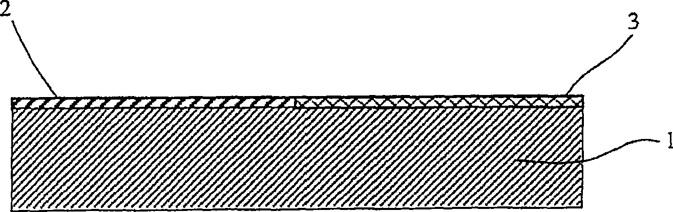
[0071] The following will refer to Figure 2a -2d, according to the first embodiment of the present invention, explain a light emitting device and a method of manufacturing the light emitting device.

[0072] In this example, MBE is used to deposit a heterostructure with an elastically strained surface layer on a substrate. exist Figure 2a A schematic cross-sectional view of the heterostructure is shown in . In this embodiment, the substrate 12 is a template substrate comprising an n-type doped GaN layer 13 grown over a sapphire substrate 14 . In this order, n-type GaN buffer layer 15 and n-type Al x Ga 1-x An N (0<x≦1) (hereinafter referred to as AlGaN) layer 16 is grown covering the substrate 12 . Because the AlGaN layer is partially or completely strained onto the GaN buffer layer 15 in a plane parallel to the substrate surface, and because the ASLP of the released AlGaN is not equal to the ASLP of the GaN buffer layer (because GaN layers grown on sapphire are usually...


PUM


Abstract

A method of manufacturing a semiconductor device comprises depositing a semiconductor layer over a semiconductor surface having at least one first region with a first (average surface lattice) parameter value and at least one second region having a second parameter value different from the first. The semiconductor layer is deposited to a thickness so self-organised islands form over both the first and second regions. The difference in the parameter value means the islands over the first region have a first average parameter value and the islands over the second region have a second average parameter value different from the first. A capping layer is deposited over islands and has a greater forbidden bandgap than the islands whereby the islands form quantum dots, which have different properties over the first and second regions due to difference(s) between the first and second region islands. The invention also relates to a semiconductor device using the method.

Description

technical field [0001] The invention relates to a semiconductor device including quantum dots, in particular to an optoelectronic semiconductor device including quantum dots and a manufacturing method thereof. The invention can be applied, for example, to light emitting diodes (LEDs) or semiconductor laser diodes. Background technique [0002] Semiconductor optoelectronic devices such as light emitting diodes (LEDs) and laser diodes (LDs) have a wide variety of applications, including as components of indicator lights, as solid state light sources, and in optical storage systems. The suitability of the device for application is determined according to the wavelength of light generated by the device. [0003] The wavelength of light emitted from an optoelectronic device is determined according to the light emitting region of the device, hereinafter referred to as the active region of the device. Typically, semiconductor light emitting devices are fabricated using epitaxial ...

Claims


Application Information

Patent Timeline
Patent Type & Authority Applications(China)
IPC IPC(8): H01L21/02H01L21/20H01L33/00H01S5/343H01L33/06
CPCB82Y10/00H01L29/2003H01L31/101H01S5/4087H01L21/02458H01L21/0254H01L21/0237H01L29/127H01S5/34333H01L21/0242H01S5/3412H01L33/06H01L21/02639B82Y20/00B82Y30/00H01L31/0352H01S5/341
Inventor 蒂姆·迈克尔·斯密顿凯瑟琳·路易斯·史密斯马修·泽维尔·先尼斯图尔特·爱德华·胡帕
Owner SHARP KK
Learn More