Chip-embedded package structure and manufacturing method thereof

A manufacturing method and packaging structure technology, applied in semiconductor/solid-state device manufacturing, electrical components, electrical solid-state devices, etc., can solve problems such as unsatisfactory use requirements, poor reliability, and low yield rate of finished products, so as to facilitate mass production , the effect of counteracting uneven stress distribution and easy processing

Active Publication Date: 2011-12-28
UNIMICRON TECH CORP
View PDF0 Cites 0 Cited by
  • Summary
  • Abstract
  • Description
  • Claims
  • Application Information

AI Technical Summary

Problems solved by technology

[0007] At present, in the packaging structure embedded with chips, the carrier board will have uneven stress between the circuit build-up layer and the non-build-up layer, so the asymmetric circuit build-up layer structure 16 of the carrier board will cause the metal carrier board to warp. As a result, production is not easy, and the finished product will also have low yield and poor reliability due to excessive board warpage
[0008] Therefore, in order to reduce the board warpage caused by single-sided build-up of the chip-embedded carrier board and improve the production yield, the carrier board made of copper or BT resin can no longer meet the use requirements.

Method used


Image

  • Chip-embedded package structure and manufacturing method thereof
  • Chip-embedded package structure and manufacturing method thereof
  • Chip-embedded package structure and manufacturing method thereof

Examples


Embodiment 1

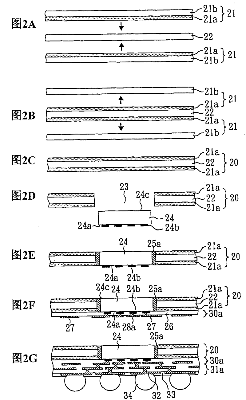
[0046] See Figure 2A to 2E , Which is a schematic cross-sectional view of the manufacturing method of the chip-embedded package structure of this embodiment.

[0047] Such as Figure 2A As shown, first, two aluminum carrier plates 21 are provided. The two aluminum carrier plates 21 can be placed in an electrolytic cell to perform anodization reaction to oxidize a surface of the aluminum carrier plate 21 to form a metal oxide layer, that is, an aluminum oxide layer 21a is formed, and the other aluminum carrier plate One part is an aluminum layer 21b. The anodizing reaction in this embodiment controls the thickness of the aluminum oxide layer by adjusting the anodizing time. Then, like Figure 2B As shown, the aluminum oxide layers 21a of the two aluminum carrier plates 21 are facing each other, and an adhesive layer 22 is sandwiched between them to make them tightly adhered. The material of the adhesive layer 22 can be thermosetting resin, and this embodiment Use epoxy resin. ...

Embodiment 2

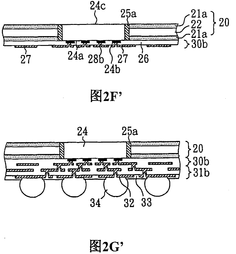
[0055] The manufacturing method of the package structure with embedded chips in this embodiment is substantially the same as that in Embodiment 1, except that the method of fixing the chip 24 to the alumina composite board is different, and the rest are the same as in Embodiment 1.

[0056] Such as image 3 As shown, the method of fixing the chip 24 to the alumina composite board 20 in this embodiment is as follows: image 3 As shown, when the chip 24 is embedded in the alumina composite board 20, epoxy resin is not used first, but when the dielectric layer 26 is laminated, the dielectric layer 26 (ie, ABF) is filled at the same time The gap between the chip 24 and the composite board opening 23 formed by the alumina composite board 20 uses the dielectric layer 26 as an adhesive material. The remaining steps are the same as in Example 1. Finally, a package structure with embedded chips of the present invention is obtained.


PUM


Abstract

The invention relates to a packaging structure with a chip embedded, and a manufacturing method thereof. The packaging structure comprises an aluminum oxide composite plate and a chip. The aluminum oxide composite plate is formed by an adhesive layer clamped between two aluminum oxide layers in an overlapping way. The chip can be embedded and fixed in the aluminum oxide composite plate, and is provided with an active surface, and the active surface is configured with a plurality of electrode pads. In addition, the invention further comprises a method for fabricating the packaging structure. The thickness of the packaging structure can be reduced, and the invention has rigidity and toughness, and provides the prefect packaging structure.

Description

Technical field [0001] The invention relates to a package structure with embedded chips and a manufacturing method thereof, in particular to a package structure with embedded chips with thin thickness, strong rigidity and toughness, and a manufacturing method thereof. Background technique [0002] With the vigorous development of the electronics industry, electronic products have gradually entered the direction of multi-functional and high-performance research and development. In order to meet the packaging requirements of high integration and miniaturization of semiconductor packages, circuit boards that provide most active and passive components and circuit connections have gradually evolved from single-layer boards to multi-layer boards, so that the In this space, the available wiring area on the circuit board is expanded through interlayer connection technology to meet the demand for high-density integrated circuits. [0003] However, in the general manufacturing process of a ...

Claims


Application Information

Patent Timeline
Patent Type & Authority Patents(China)
IPC IPC(8): H01L23/12H01L23/13H01L23/14H01L23/498H01L21/58H01L21/60
CPCH01L2224/12105
Inventor 贾侃融许诗滨
Owner UNIMICRON TECH CORP
Why Eureka
Try Eureka