
Optoelectronic component and manufacturing method

A technology of photoelectric components and electrodes, which is applied in the direction of electrical components, circuits, semiconductor devices, etc., and can solve problems such as increasing the luminous efficiency of light-emitting components, increasing the brightness of light sources, and limiting luminous efficiency

Active Publication Date: 2009-03-18
EPISTAR CORP
View PDF4 Cites 0 Cited by
  • Summary
  • Abstract
  • Description
  • Claims
  • Application Information

AI Technical Summary

Problems solved by technology

However, in the above-mentioned known technologies, the luminous effect produced is limited. Therefore, the present invention mainly discloses a compound layer of Group V / Group II added to the buffer layer of the light-emitting element, and the combination has irregular and high and low fluctuations. The shape of the active layer makes it possible to increase the brightness of the light source generated by the light-emitting area in the photoelectric element, and can increase the luminous efficiency of the light-emitting element

Method used

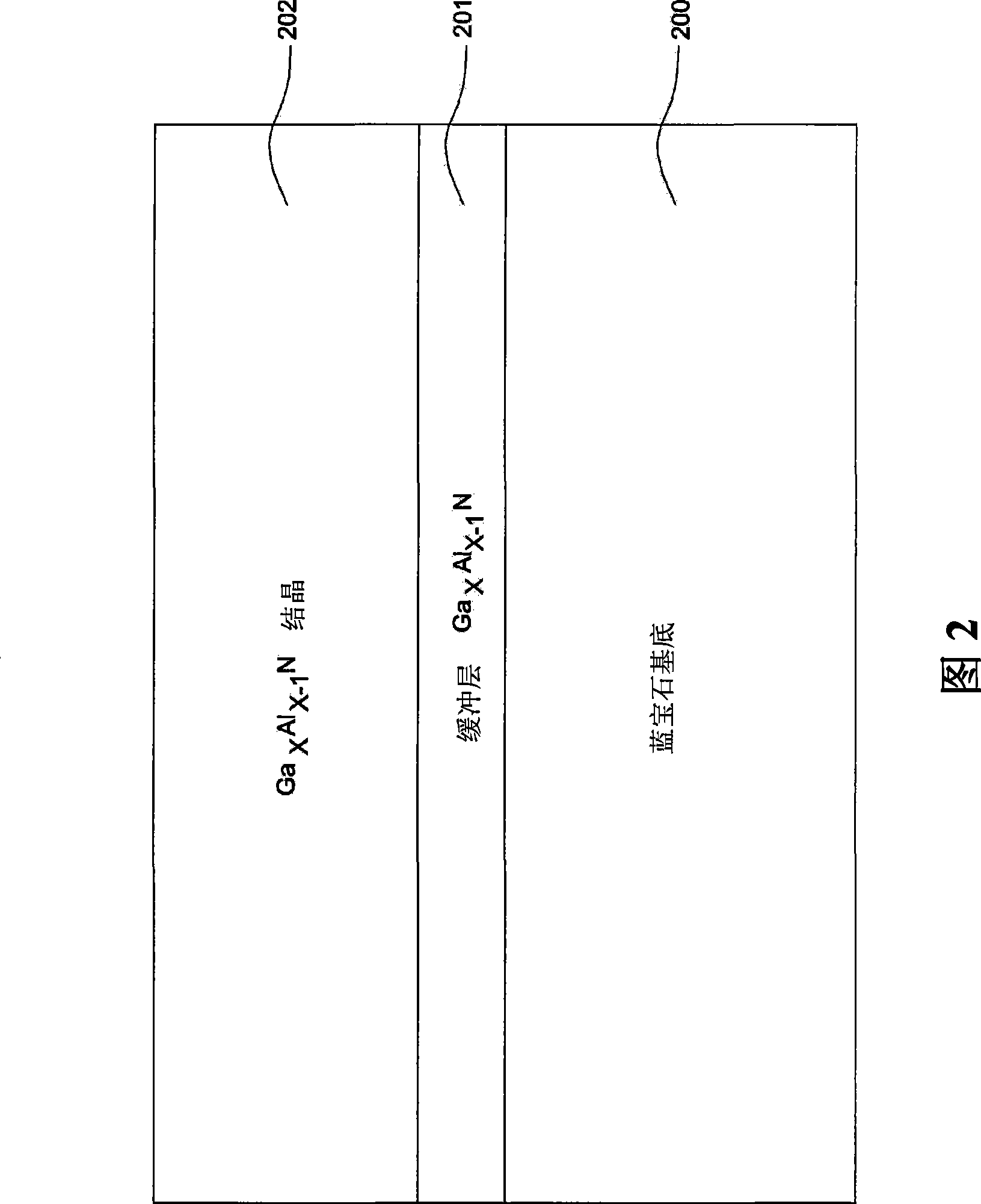
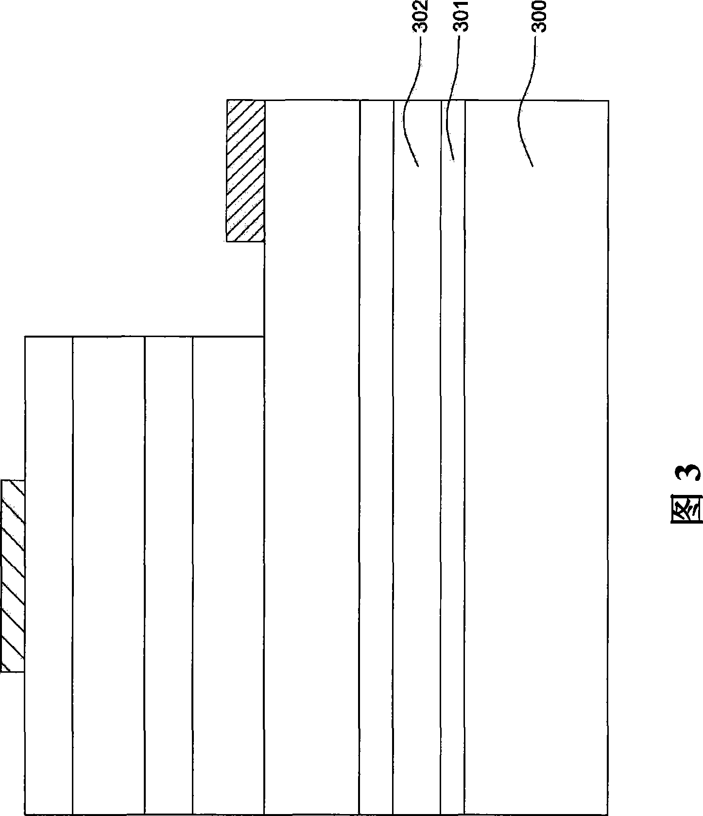

Image

  • Optoelectronic component and manufacturing method
  • Optoelectronic component and manufacturing method
  • Optoelectronic component and manufacturing method

Examples


Embodiment Construction

[0028] The direction of the present invention discussed here is a photoelectric element and its manufacturing method. In order to provide a thorough understanding of the present invention, the detailed structure of the photovoltaic element and its steps will be presented in the following description. Clearly, the practice of the present invention is not limited to specific details well known to those skilled in the art of optoelectronic components, however, a preferred embodiment of the present invention will be described in detail below. In addition to these detailed descriptions, the present invention can also be widely implemented in other embodiments, and the scope of the present invention is not limited. Without departing from the spirit and scope of the present invention, some changes and improvements can be made, Therefore, the scope of patent protection of the present invention must be determined by the appended claims of this specification.

[0029] First please refe...


PUM


Abstract

The invention provides an opto-electronic element, which comprises a fist electrode, a substrate which is formed on the first electrode and a buffer layer which is formed on the substrate, wherein the buffer layer comprises a first nitrogen-containing compound layer which is formed on the substrate, a second nitrogen-containing compound, and a V-group / II-group compound layer which is formed between the first nitrogen-containing compound layer and the second nitrogen-containing compound layer, then a first semiconductor conductive layer is formed on the buffer layer, an active layer is formed on the first semiconductor conductive layer, wherein the active layer is provided with a plurality of irregular multi-layer quantum wells with uneven shapes, a second semiconductor is formed on the active layer, a transparent conductive layer is formed on the second conductive layer, and a second electrode is formed on the transparent conductive layer.

Description

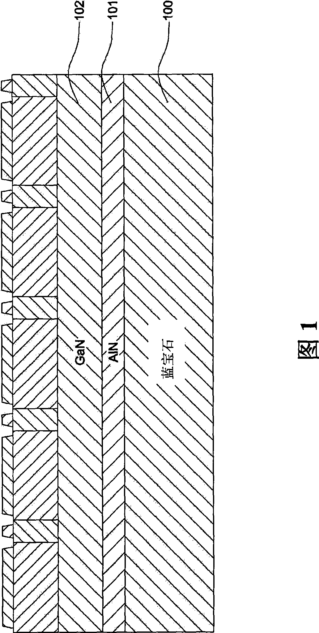
technical field [0001] The present invention mainly discloses a photoelectric element, and more particularly discloses an epitaxial stack structure of a photoelectric element having a Group V / Group II buffer layer. Background technique [0002] In order to improve the crystal quality of the GaN compound layer, it is necessary to solve the problem of lattice matching between sapphire and the GaN compound layer as the light emitting layer. Therefore, in the known technology, for example, US Pat. No. 5,122,845 (as shown in FIG. 1 ), a buffer layer (buffer layer) 101 mainly composed of aluminum nitride (AlN) is formed between the substrate 100 and the gallium nitride layer 102 , and the crystal structure of the buffer layer 101 is microcrystalline or polycrystalline and mixed in the state of amorphous silicon, so that the crystal structure of the buffer layer 101 can be improved between the gallium nitride compound layer 103 The problem of crystal mismatching between them. As ...

Claims


Application Information

Patent Timeline
Patent Type & Authority Applications(China)
IPC IPC(8): H01L33/00H01L33/06H01L33/12
Inventor 蔡宗良李玉柱
Owner EPISTAR CORP
Learn More