Array substrate of LCD
A liquid crystal display and array substrate technology, applied in the field of liquid crystal display device manufacturing, can solve the problems of reducing the aperture ratio, light leakage, unable to completely prevent the light leakage phenomenon, etc., and achieve the effect of reducing the area of light leakage and reducing the distance
- Summary
- Abstract
- Description
- Claims
- Application Information
AI Technical Summary
Problems solved by technology
Method used
Image

Examples
Embodiment Construction
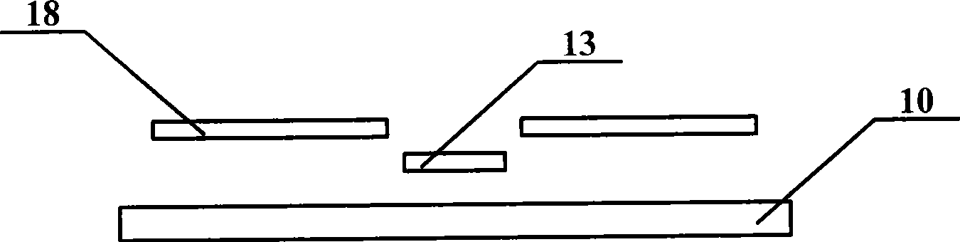
[0014] Such as image 3 Shown is a schematic cross-sectional structure diagram of the data line direction of the first embodiment of the array substrate of the liquid crystal display of the present invention. This embodiment includes a substrate 10, on which several gate lines (not shown) and data lines 13 intersecting each other to define a pixel area are arranged, and the pixel area is provided with pixel electrodes 18, and the pixel electrodes 18 are connected to each other. The distance is 2-6 μm. In this embodiment, the distance between the pixel electrodes 18 can be further reduced to 2-4 μm.
[0015] In this embodiment, the distance between the pixel electrodes is minimized, that is, set to 2-4 μm, thereby reducing the distance between the pixel electrodes and the data lines, and effectively reducing the area where light leakage may occur when the panel is tapped.
[0016] As the horizontal distance between the pixel electrode and the data line decreases, the capacita...
PUM
 Abstract
Description
Claims
Application Information
 - R&D
- Intellectual Property
- Life Sciences
- Materials
- Tech Scout
- Unparalleled Data Quality
- Higher Quality Content
- 60% Fewer Hallucinations
Browse by: Latest US Patents, China's latest patents, Technical Efficacy Thesaurus, Application Domain, Technology Topic, Popular Technical Reports.
© 2025 PatSnap. All rights reserved.Legal|Privacy policy|Modern Slavery Act Transparency Statement|Sitemap|About US| Contact US: help@patsnap.com