Quantum dot light emitting devices

A technology of electroluminescent element and manufacturing method, which is applied to the manufacturing of electroluminescent light sources, electrical components, semiconductor/solid-state devices, etc. Life characteristics, effect of improving light emission characteristics

Inactive Publication Date: 2009-05-06
DAI NIPPON PRINTING CO LTD
View PDF10 Cites 37 Cited by
  • Summary
  • Abstract
  • Description
  • Claims
  • Application Information

AI Technical Summary

Problems solved by technology

[0019] However, no one has proposed a method of patterning the light-emitting layer using the above-mentioned quantum dot film formation.

Method used


Image

  • Quantum dot light emitting devices
  • Quantum dot light emitting devices
  • Quantum dot light emitting devices

Examples


no. 1 Embodiment approach

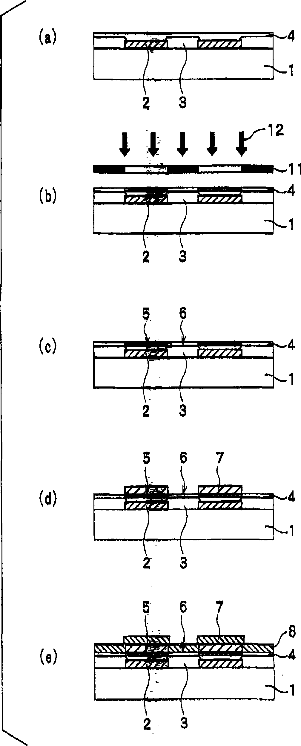
[0055] The first embodiment of the manufacturing method of the EL element of the present invention is characterized in that it includes the following steps: a wettability changing layer forming step of forming a wettability layer containing a photocatalyst on the substrate on which the first electrode layer is formed. The wettability changing layer whose properties are changed by the action of the photocatalyst accompanied by energy irradiation; the wettability changing pattern forming step, by irradiating the above wettability changing layer in a pattern shape, the above wettability changing layer A wettability change pattern consisting of a lyophilic region and a liquid-repellent region is formed on the surface; a light-emitting layer forming step is to apply a coating for forming a light-emitting layer containing quantum dots with ligands arranged around it on the above-mentioned lyophilic region. Distribute the liquid to form a luminescent layer.

[0056] A method of manuf...

no. 2 Embodiment approach

[0334] The second embodiment of the manufacturing method of the EL element of the present invention is characterized in that it includes the step of forming a wettability variable layer on the substrate on which the first electrode layer is formed, forming a wettability factor accompanying energy irradiation. The wettability changing layer changed by the action of the photocatalyst; the wettability changing pattern forming process, relative to the above wettability changing layer, vacates the gap that can be affected by the action of the catalyst accompanying energy irradiation, and arranges it on the substrate. A photocatalyst treatment layer substrate having a photocatalyst treatment layer containing at least a photocatalyst is formed, and then, by irradiating energy in a pattern, a wettability region consisting of a lyophilic region and a liquid repellent region is formed on the surface of the wettability changing layer. Moisture change pattern; light emitting layer forming ...

Embodiment 1

[0482] (Formation of transparent electrodes)

[0483] On the cleaned glass substrate, use sputtering method to 1500 The film thickness forms an ITO film as a transparent electrode. Then, the ITO film was patterned with a line width of 300 μm and a space of 100 μm by photolithography.

[0484] (Formation of insulating layer)

[0485] A negative resist (manufactured by Nippon Steel Chemical Co., Ltd., V259PA) was applied by spin coating to a dry film thickness of 1 μm on the substrate on which the ITO film was patterned, and then baked at 120° C. for 1 hour. Then, a 365-nm UV light was exposed at an exposure amount of 500 mJ through a photomask with a width of 100 μm centering on the space portion without the ITO film. At this time, exposure was performed with a gap of 1 mm between the photomask and the substrate. This was developed for 40 seconds using an organic alkali developer (manufactured by Nippon Steel Chemical Co., Ltd., V259OD), and then baked at 160° C. for 1 hou...


PUM

PropertyMeasurementUnit
wavelengthaaaaaaaaaa
particle sizeaaaaaaaaaa
thicknessaaaaaaaaaa

Abstract

A primary object of this invention is to provide a manufacturing method for an EL element, which can facilitate patterning for a luminescent layer containing quantum dots. This method includes: a wettability-changing-layer-forming step for forming a wettability changing layer containing a photocatalyst, on a substrate having a first electrode layer formed thereon, wherein wettability of the wettability-changing layer is changed by an effect of the photocatalyst associated with irradiation with energy; and a wettability-changing-pattern forming step for forming a wettability changing pattern composed of lyophilic regions and liquid-repellent regions, on a surface of the wettability changing layer, by irradiating the wettability changing layer with energy in a patterning manner. Additionally, in this method, a luminescent layer is formed onto each lyophilic region, by coating a luminescent-layer-forming coating liquid containing the quantum dots, around each of which ligands are attached. In this way, the EL element can be obtained.

Description

[0001] References to related applications [0002] This patent application enjoys the priority of Japanese application Japanese Patent Application No. 2007-256852 filed on March 28, 2007. The entire disclosure content of this prior application constitutes a part of this specification by reference. technical field [0003] The present invention relates to a method for manufacturing an electroluminescence (hereinafter sometimes abbreviated as EL) element by patterning a light-emitting layer containing quantum dots using a layer whose wettability is changed by the action of a photocatalyst accompanying energy irradiation and the method. The produced EL element. Background technique [0004] The EL element is a kind of element in which holes and electrons injected from two opposite electrodes are combined in the light-emitting layer, and the light-emitting material in the light-emitting layer is excited according to its energy, thereby emitting light corresponding to the color ...

Claims


Application Information

Patent Timeline
Patent Type & Authority Applications(China)
IPC IPC(8): H01L51/56H01L51/50
CPCH01L51/5012H01L51/0003H01L51/0012B82Y20/00B82Y30/00H10K71/191H10K71/12H10K50/11H10K71/00H05B33/10H05B33/22
Inventor 饭泉安广下河原匡哉
Owner DAI NIPPON PRINTING CO LTD
Why Eureka
Try Eureka