Low-noise wide-band amplifier circuit

An amplifier circuit and low-noise technology, applied in the field of circuits, can solve the problems of not meeting the requirements of technological development, poor anti-kickback ability, large noise figure, etc., and achieve high gain, low power consumption, and good isolation effect

Inactive Publication Date: 2009-05-06
RDA TECH
View PDF0 Cites 9 Cited by
  • Summary
  • Abstract
  • Description
  • Claims
  • Application Information

AI Technical Summary

Problems solved by technology

[0006] The above-mentioned three kinds of existing low-noise broadband amplifier circuits generally have the disadvantages of large noise...

Method used


Image

  • Low-noise wide-band amplifier circuit
  • Low-noise wide-band amplifier circuit
  • Low-noise wide-band amplifier circuit

Examples


Embodiment Construction

[0015] Such as Figure 4 As shown, the low-noise broadband amplifier circuit of the present invention includes a first-stage circuit and a second-stage circuit, the first-stage circuit includes two inverters, and the two ends of the differential input signal are respectively connected to the two inverters The input terminals INP and INN of the device, the second stage circuit also includes two inverters, the output terminals of the two inverters of the first stage circuit are respectively connected to the two inverters of the second stage circuit The input end of the phase converter, the first stage circuit is isolated from the second stage circuit by a current source, and a current source is also isolated between the second stage circuit and the power supply, and the two stages of the second stage circuit The output terminals VOP and VON of each inverter are the output terminals of the low-noise broadband amplifier circuit.

[0016] Coupling capacitors C3 and C4 are provided...


PUM


Abstract

The invention discloses a circuit of a low-noise broadband amplifier, which comprises a first-stage circuit and a second-stage circuit, wherein the first-stage circuit comprises two phase inverters. Both ends of a differential input signal are respectively connected with the input ends of the two phase inverters. The second-stage circuit also comprises two phase inverters. The output ends of the two phase inverters of the first-stage circuit are respectively connected with the input ends of the two phase inverters of the second-stage circuit. The first-stage circuit and the second-stage circuit are isolated by a current source, the second-stage circuit and a power supply are also isolated by a current source, and the output ends of the two phase inverters of the second-stage circuit are the output ends of the circuit of a low-noise broadband amplifier. The invention uses the two-pole structure of current multiplexing and has excellent stability and high gain performance, and the power consumption is also greatly reduced; the second-stage circuit has the effect of resisting the reverse kick of a back loading circuit, and higher gain is realized.

Description

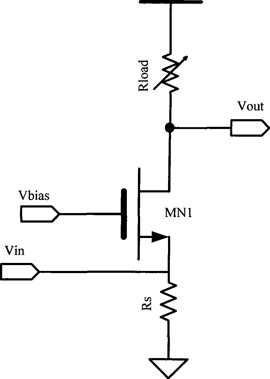
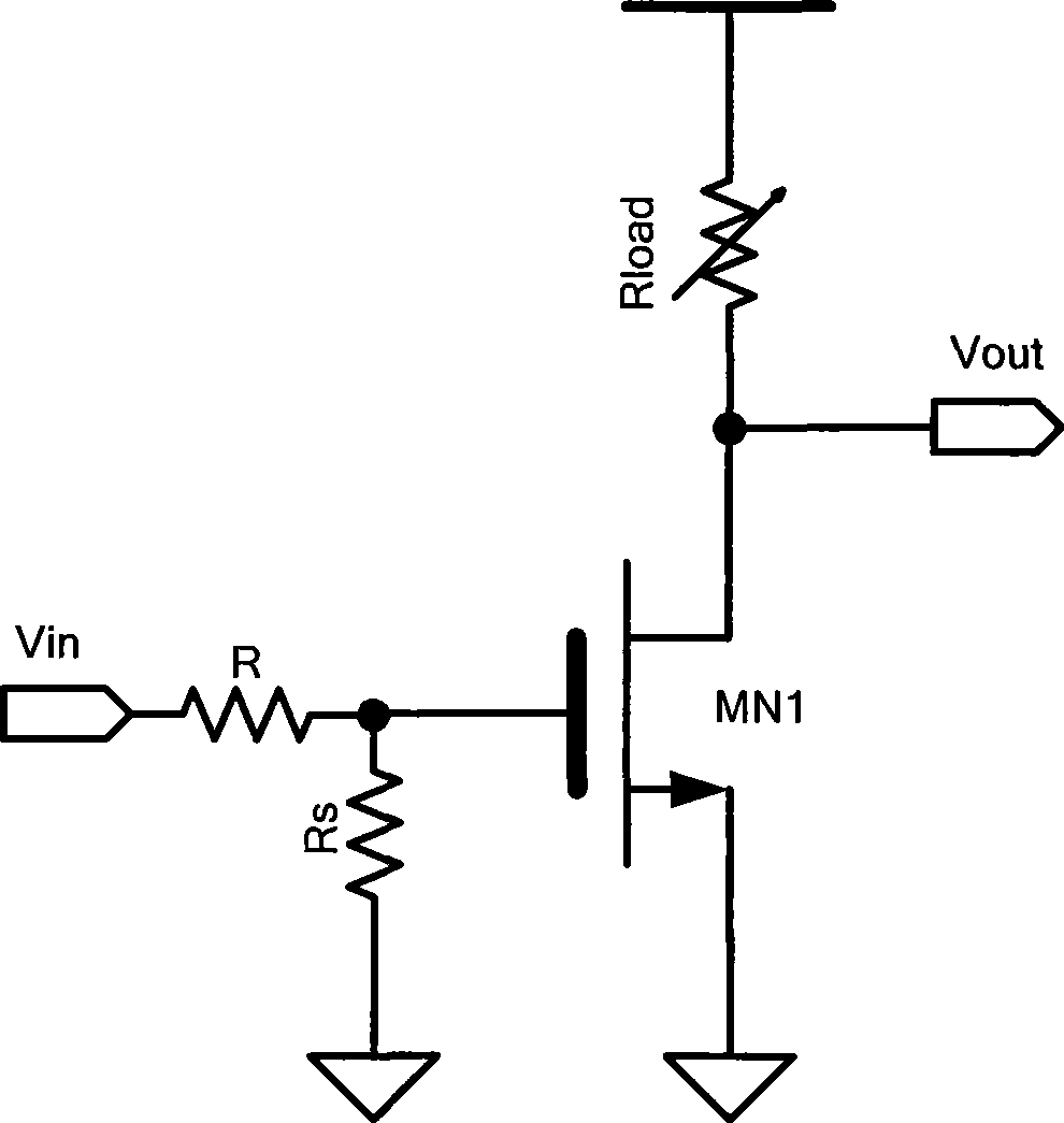
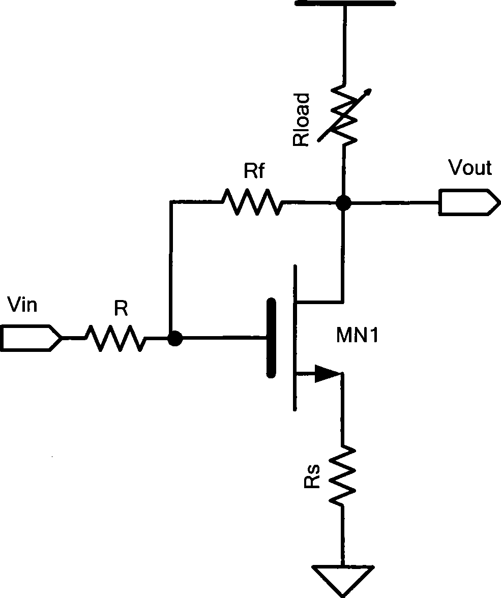
technical field [0001] The invention relates to a circuit, especially a low-noise broadband amplifier circuit. Background technique [0002] The low-noise broadband amplifier circuit is the front-end module of the RF chip, which requires the characteristics of low noise, high bandwidth, high linearity, high gain, and low power consumption. It is mostly used in FM demodulators, TV demodulators, UWB or other broadband radio frequency in the technical plan. Among the existing low-noise broadband amplifier (LNA) circuit schemes, there are three common ones: [0003] figure 1 The circuit shown is a low-noise broadband amplifier circuit with a common-gate input structure, including an NMOS transistor. The gate of the NMOS transistor is connected to a bias voltage Vbias, the drain is connected to the power supply terminal through a variable resistor Rload, and the source is The resistor Rs is grounded, the end of the resistor Rs connected to the source is used as a signal input ...

Claims


Application Information

Patent Timeline
IPC IPC(8): H03F1/26H03F1/42H03F3/193H03K19/20H03K19/0944
Inventor 赵春魏述然
Owner RDA TECH
Why Eureka
Try Eureka