Method for in-situ preparation of self-supporting gallium nitride underlay

A gallium nitride substrate, in-situ technology, applied in gaseous chemical plating, semiconductor/solid-state device manufacturing, coating, etc., can solve the problems of increasing cost and complexity, and achieve the effect of increasing cost and good quality

Inactive Publication Date: 2009-05-13
NANJING UNIV
View PDF1 Cites 5 Cited by
  • Summary
  • Abstract
  • Description
  • Claims
  • Application Information

AI Technical Summary

Problems solved by technology

However, because the laser stripping method requires a short-wavelength laser, and the irradiation power and

Method used


Image

  • Method for in-situ preparation of self-supporting gallium nitride underlay

Examples


Embodiment 1

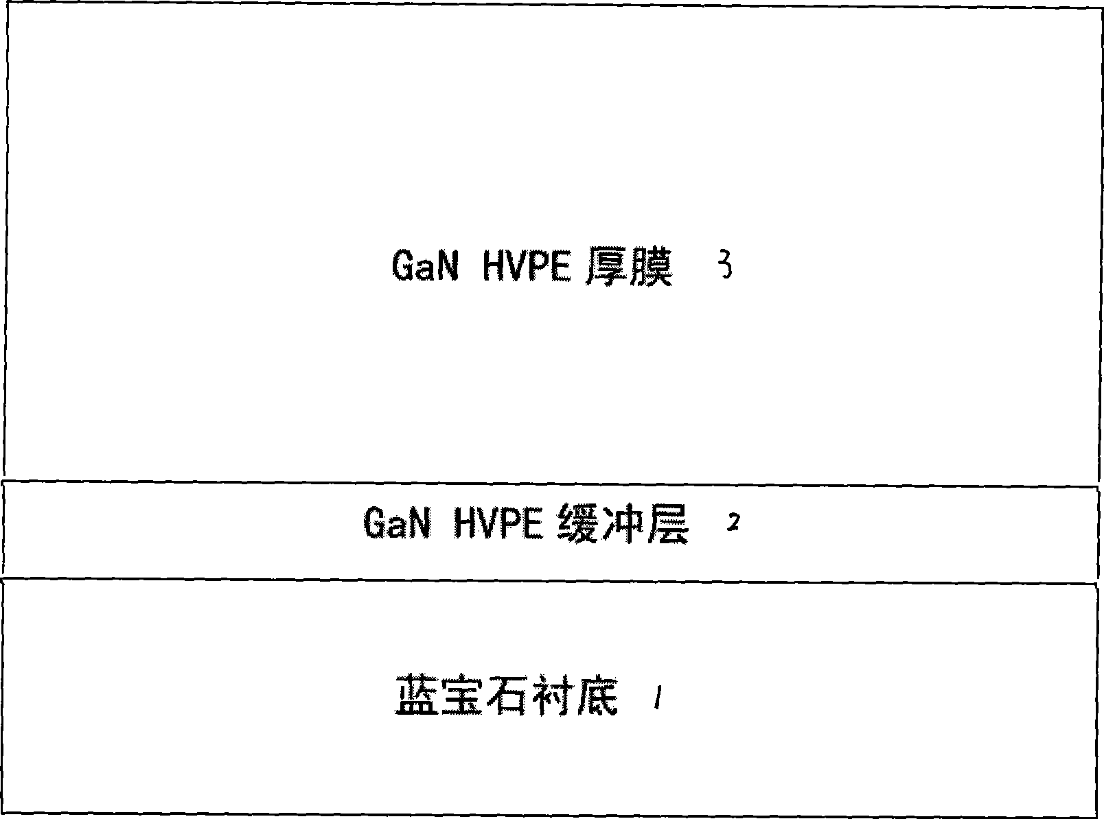
[0021] Horizontal HVPE system, the growth temperature of the buffer layer is 700°C, and the growth time of the buffer layer is 1 minute. Buffer layer growth conditions, ammonia and HCl as gas source, NH 3 The flow rate is 1000 sccm, the ammonia carrier gas flow rate is 500 sccm, the HCl flow rate is 10 sccm, the HCl carrier gas flow rate is 200 sccm, and the total nitrogen gas flow rate is 1000 sccm. Raise the temperature to 1050°C to grow a GaN thick film for about 2 hours with a thickness of 200-300 microns. Growth conditions NH 3 The flow rate is 1000 sccm, the ammonia carrier gas flow rate is 500 sccm, the HCl flow rate is 20 sccm, the HCl carrier gas flow rate is 200 sccm, and the total nitrogen gas flow rate is 2500 sccm.

[0022] After the growth is completed, the temperature is lowered. The direct cooling method is adopted, and the cooling rate is about 10°C / min. The result is a GaN self-supporting substrate of nearly 2 inches and more than 200 microns thick.


PUM


Abstract

The invention relate to a method for preparing a self-supporting gallium nitride substrate at the home position. A GaN buffer layer film grows on a sapphire in a HVPE growth mode; a reaction source material is gallium metal, highly pure HCl or trimethyl gallium or other organic gallium sources; and the carrier gas is N2 and NH3. The growth temperature is 550 to 750 DEG C; and the thickness of the buffer layer is 50nm to1mu m. When the growth of the buffer layer is completed, the HCl gas or trimethyl gallium gas is closed; the temperature is increased under the protection of ammonia gas to reach 1,000 to 1,100 DEG C within 15+-4 minutes; and GaN starts to grow till reaching the required thickness. The HCl gas is closed to stop the growth; the temperature is decreased under the protection of ammonia gas, and the temperature fall rate is maintained between 5 and 20 DEG C/min; and the temperature fall mode is to maintain the temperature for 10 to 30 minutes when the temperature is reduced to 650 to 750 DEG C and then to naturally cool down to a room temperature so as to obtain the self-peeling self-supporting GaN substrate.

Description

1. Technical field [0001] The invention relates to a method and technology for growing a GaN thick film by HVPE on a sapphire substrate by using a low-temperature GaN HVPE buffer layer and a special cooling process, and obtaining a self-supporting GaN substrate in situ. 2. Background technology [0002] Group III-V nitride materials (also known as GaN-based materials) mainly based on GaN, InGaN, and AlGaN alloy materials are new semiconductor materials that have attracted much attention in the world in recent years. Its 1.9-6.2eV continuously variable direct band gap, excellent physical and chemical stability, high saturation electron drift velocity, high breakdown field strength and high thermal conductivity and other superior properties make it the best choice for the preparation of short-wavelength semiconductor optoelectronic devices and high-frequency, high-voltage, high-temperature microelectronic devices Material. [0003] Due to the limitations of the physical prope...

Claims


Application Information

Patent Timeline
IPC IPC(8): C23C16/34C23C16/455H01L21/00
Inventor 修向前张荣华雪梅陆海谢自力顾书林施毅朱顺明韩平胡立群郑有炓
Owner NANJING UNIV
Why Eureka
Try Eureka