Hybrid integrated circuit structure of three-dimensional CMOS and molecule switching element

A hybrid integrated circuit and molecular switch technology, applied in circuits, semiconductor devices, electrical solid state devices, etc., can solve problems that are not well solved, and achieve the effects of increased speed, simplified manufacturing process, and improved integration

Inactive Publication Date: 2009-05-13
INST OF MICROELECTRONICS CHINESE ACAD OF SCI
View PDF0 Cites 5 Cited by
  • Summary
  • Abstract
  • Description
  • Claims
  • Application Information

AI Technical Summary

Problems solved by technology

Since the upper and lower electrodes of molecular switching devices are not on the same plane, how to prepare these through holes and how to avoid the influence between the through holes and the upper and lower electrodes have not been well resolved.

Method used


Image

  • Hybrid integrated circuit structure of three-dimensional CMOS and molecule switching element
  • Hybrid integrated circuit structure of three-dimensional CMOS and molecule switching element
  • Hybrid integrated circuit structure of three-dimensional CMOS and molecule switching element

Examples


Embodiment Construction

[0027] In order to make the object, technical solution and advantages of the present invention clearer, the present invention will be described in further detail below in conjunction with specific embodiments and with reference to the accompanying drawings.

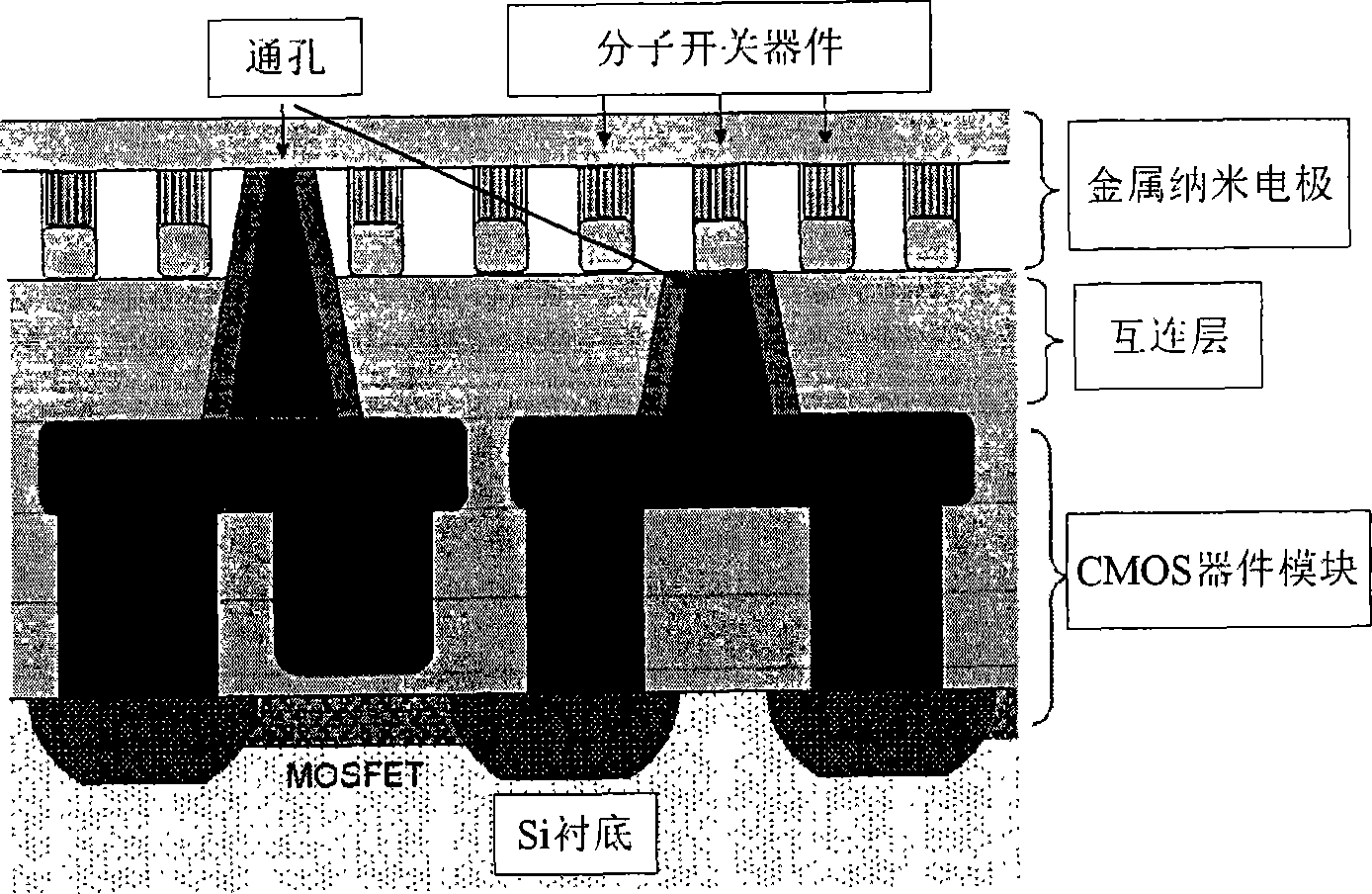
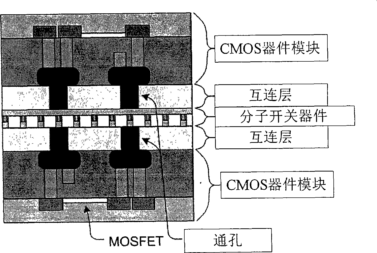
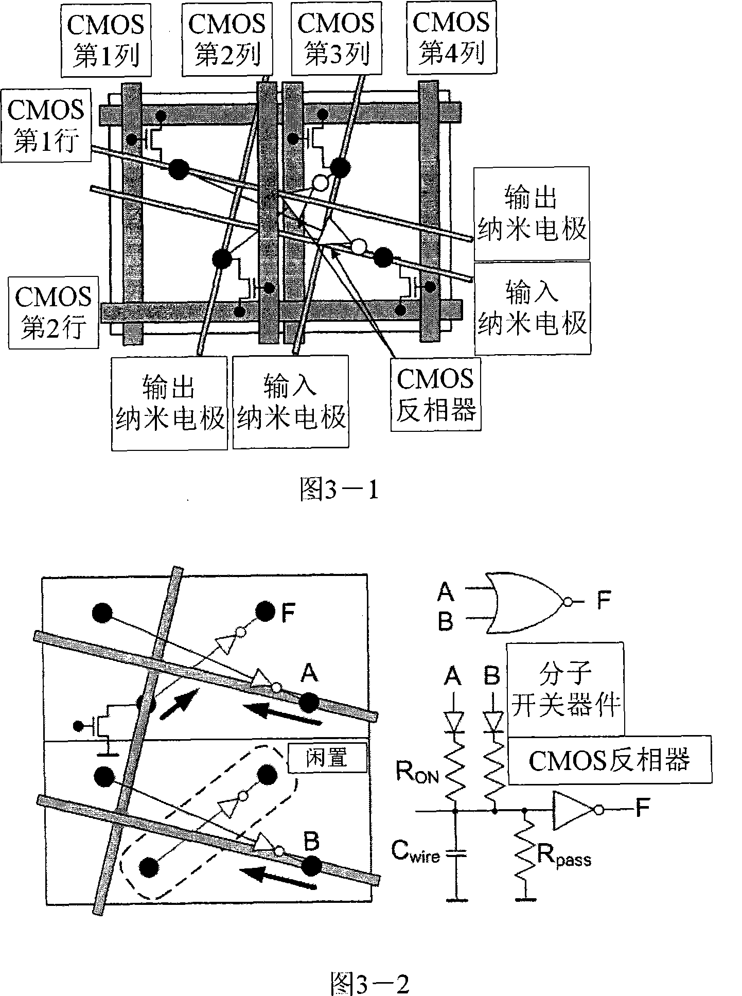
[0028] The present invention provides a hybrid integrated circuit of a three-dimensional CMOS and a molecular switch device (CMOL). The electrodes are respectively connected with the upper and lower corresponding CMOS devices to form a three-dimensional structure.

[0029] Such as figure 2 as shown, figure 2 A schematic diagram of a hybrid integrated circuit structure of a three-dimensional CMOS and molecular switching device provided by the present invention; wherein, the upper and lower electrodes of the molecular switching device are respectively connected to the top and bottom CMOS devices, and then bonded to form a three-dimensional structure.

[0030] figure 2 The hybrid integrated circuit structure of the thr...


PUM


Abstract

The invention relates to the technical field of nanometer circuit structures in microelectronics and molectronics, which discloses a three-dimensional hybrid integrated circuit structure of a CMOS and a molecular switch device. The structure is formed by sequentially connecting a CMOS device as a top layer, a molecular switch device and a CMOS device as a bottom layer from the top to the bottom; the CMOS device at the top layer is connected with an electrode on the molecular switch device by a through hole, the CMOS device at the bottom layer is connected with an electrode below the molecular switch device by a through hole, and the CMOS device at the top layer and the CMOS device at the bottom layer are bonded together. The invention avoids the influence on the upper electrode and the lower electrode by the through holes which are not on the same surface. Meanwhile, the circuit integration is increased by once, and the invention has higher creative meaning and practical value.

Description

technical field [0001] The invention relates to the technical field of nanometer circuit structure in microelectronics and molecular electronics, in particular to a hybrid integrated circuit structure of three-dimensional CMOS and molecular switch devices. Background technique [0002] As the feature size of large-scale integrated circuits enters the nanometer level, the traditional silicon-based integrated circuit technology is facing challenges, and the research on new materials and new structures has become a hot spot. Molecular electronic devices, one of the branches of nanoelectronics, are booming. [0003] Crossover molecular electronic devices based on bistable switching characteristics (Chen Y, Jung G Y, Ohlberg D AA et al. Nanotechnology, 2003, 14: 462) are currently one of the main structures of molecular electronic devices and have received extensive attention. A crossover molecular electronic device is a two-terminal device, as opposed to a conventional three-ter...

Claims


Application Information

Patent Timeline
Patent Type & Authority Applications(China)
IPC IPC(8): H01L25/16H01L27/02H01L23/522
Inventor 涂德钰刘明王慰商立伟谢常青
Owner INST OF MICROELECTRONICS CHINESE ACAD OF SCI
Why Eureka
Try Eureka