Method for pre-aligning silicon chip

A pre-alignment, silicon wafer technology, applied in the photoengraving process, optics, instruments and other directions of the pattern surface, can solve the problems of accuracy impact, strict measurement requirements, difficulties, etc., to improve accuracy, improve precision, improve Precise and efficient effects

Active Publication Date: 2009-05-20
SHANGHAI MICRO ELECTRONICS EQUIP (GRP) CO LTD
View PDF1 Cites 39 Cited by
  • Summary
  • Abstract
  • Description
  • Claims
  • Application Information

AI Technical Summary

Problems solved by technology

[0004] Among the general methods for calculating the centroid of silicon wafers, the calculation amount of the radius of gyration method is small, but the requirements for measurement are very strict. The amount is small, but the accuracy is affected by the measurement noise. In addition, there are certain difficulties in judging the gap, and the error itself is relatively large.
The calculus centroid method is used to calculate the centroid. Its advantage is that it is suitable for the calculation of the geometric center of graphics of any shape. The disadvantage is that it needs to collect enough edge collection points.
[0005] In addition, in the calculation of the centroid of the silicon wafer, the collected data of the gap is usually discarded, and the starting point and the end point of the gap are directly used to calculate the centroid of the silicon wafer; or the gap data is compensated, but whether it is discarded or It is the usual compensation method, and the data of the gap is not realistic and accurate enough
[0006] Before locating the notch on the silicon wafer, the methods commonly used for rough positioning of the notch include: cross-correlation detection method, cosine curve fitting method, and edge change rate method, but none of them are ideal. For example, the edge change rate method is used to rough the gap Positioning has great limitations. For example, in Chinese patent: CN1787200A, the included angle is calculated for three adjacent sampling points, and an appropriate threshold value is required to be set. This threshold value is determined by empirical methods. The situation is very unstable. This method requires that the edge data of the silicon wafer collected by the CCD must be evenly distributed, and the amplitude of the adjacent data collected cannot change too much. If the pre-alignment of the silicon wafer is not very circular , the experiment proves that due to the uneven rotation speed of the rotary table, the control program written by the algorithm using this idea is prone to collapse, and the center of the lowest point of the silicon wafer gap cannot be found or found incorrectly, which will have an adverse effect on the orientation of the silicon wafer. A good impact will eventually lead to a significant reduction in the overall performance of the lithography machine manufacturing equipment assembly line and the production yield

Method used


Image

  • Method for pre-aligning silicon chip
  • Method for pre-aligning silicon chip
  • Method for pre-aligning silicon chip

Examples


Embodiment Construction

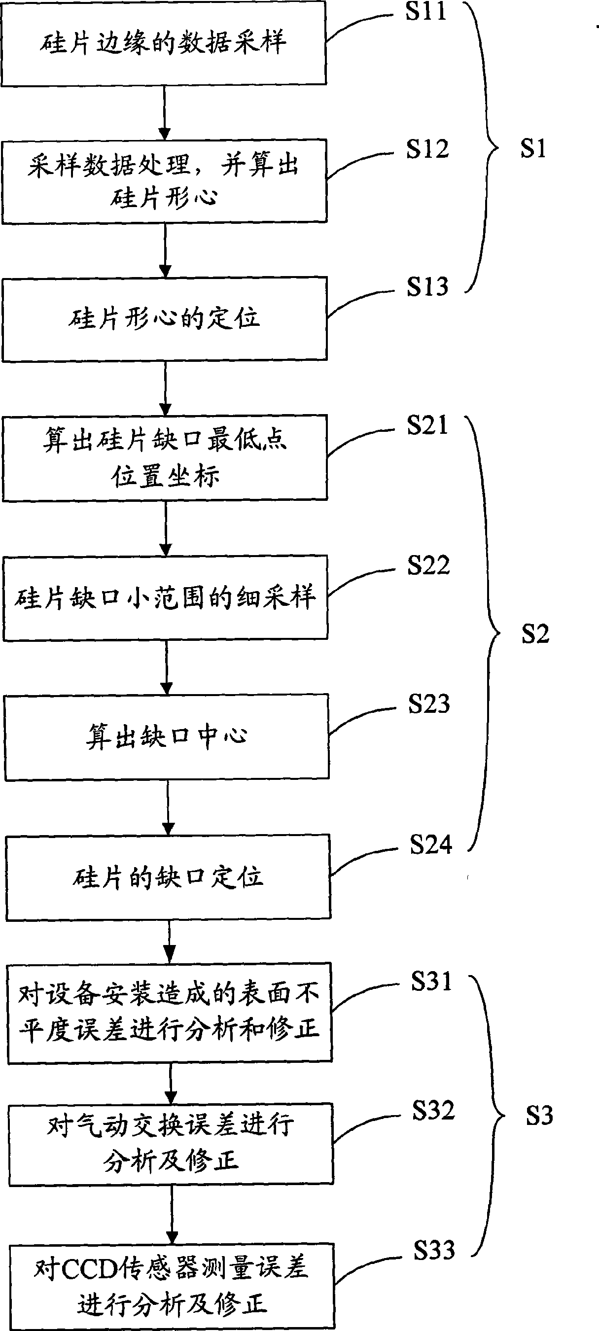
[0027] The implementation of the present invention is described below through specific examples, and those skilled in the art can easily understand other advantages and effects of the present invention from the contents disclosed in this specification. The present invention can also be implemented or applied through other different specific embodiments, and various modifications and changes can be made to the details in this specification based on different viewpoints and applications without departing from the spirit of the present invention.

[0028] The silicon chip pre-alignment method described in the present invention can be applied to the silicon chip exposure process of the photolithography machine in the microelectronic device manufacturing industry.

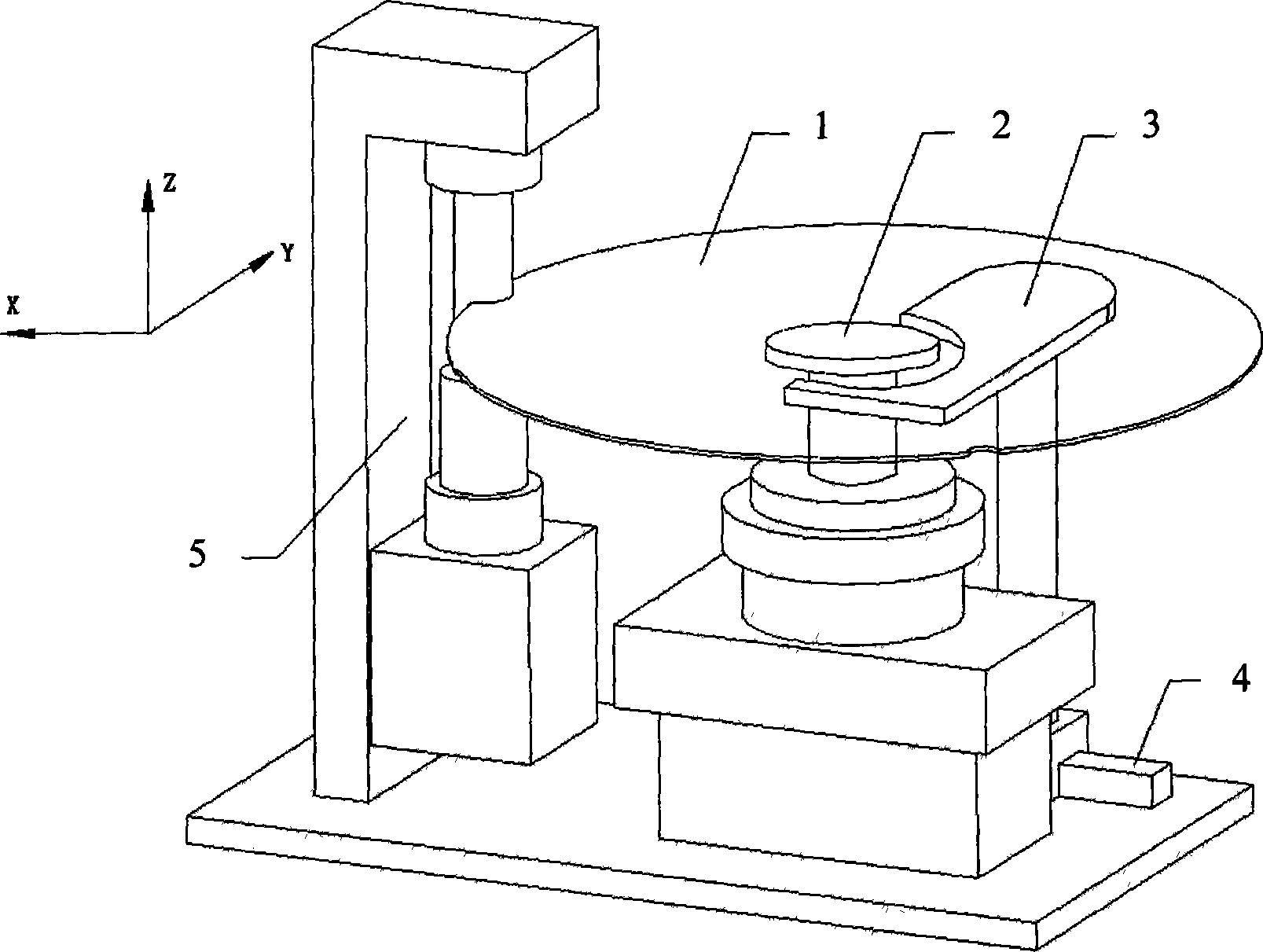
[0029] figure 1 It is a structural diagram of the mechanical equipment of the silicon wafer pre-alignment device of the lithography machine. As shown in the figure, the silicon wafer pre-alignment device has a rotary ta...


PUM


Abstract

The invention provides a method for pre-aligning a silicon chip. The method improves accuracy and efficiency of pre-aligning the silicon chip on several aspects of optimizing control, error compensation, and the like. The method comprises the following steps: preliminarily positioning a gap by adopting a stepping fall method, and calculating a lowest position of the gap by adopting a reference method; and compensating data for collection points of the gap, and calculating a form center of the silicon chip by applying a mode of matrix fitting. Therefore, the method improves calculation accuracy of the form center to a great extent, only needs once data sampling of a CCD linear sensor to position accurately, and improves pre-aligning accuracy and efficiency. In addition, through correcting pre-aligning error to correct calculation error of the form center of the silicon chip, the method further improves the pre-aligning accuracy.

Description

technical field [0001] The invention relates to a silicon chip pre-alignment method, in particular to a silicon chip pre-alignment method applied in a photolithography machine. Background technique [0002] The photolithography machine is an indispensable tool in the manufacturing of microelectronic devices, and because the field of view of the photolithography machine is very small, before the silicon wafer is transferred to the photolithography machine for exposure, the silicon wafer must be pre-aligned, so that the transmission The silicon wafer on the exposure table is within the field of view of the lithography machine, so pre-alignment of the silicon wafer is an important part of the silicon wafer exposure performed by the lithography machine. Specifically, pre-alignment is a precise positioning for transporting the silicon wafer to the workpiece table for exposure, and the pre-alignment directly affects the exposure accuracy of the silicon wafer and the working effici...

Claims


Application Information

Patent Timeline
Patent Type & Authority Applications(China)
IPC IPC(8): G03F7/20G03F9/00
Inventor 王科
Owner SHANGHAI MICRO ELECTRONICS EQUIP (GRP) CO LTD
Why Eureka
Try Eureka