

Induction coupling plasma processing apparatus and method
A technology of plasma and inductive coupling, which is applied in plasma, semiconductor/solid-state device manufacturing, gaseous chemical plating, etc., can solve the problems of high device cost, high power cost, and large power loss, and achieve high device cost , The effect of increasing the cost of electricity
- Summary
- Abstract
- Description
- Claims
- Application Information
AI Technical Summary
Problems solved by technology
Method used
Image



Examples
Embodiment Construction
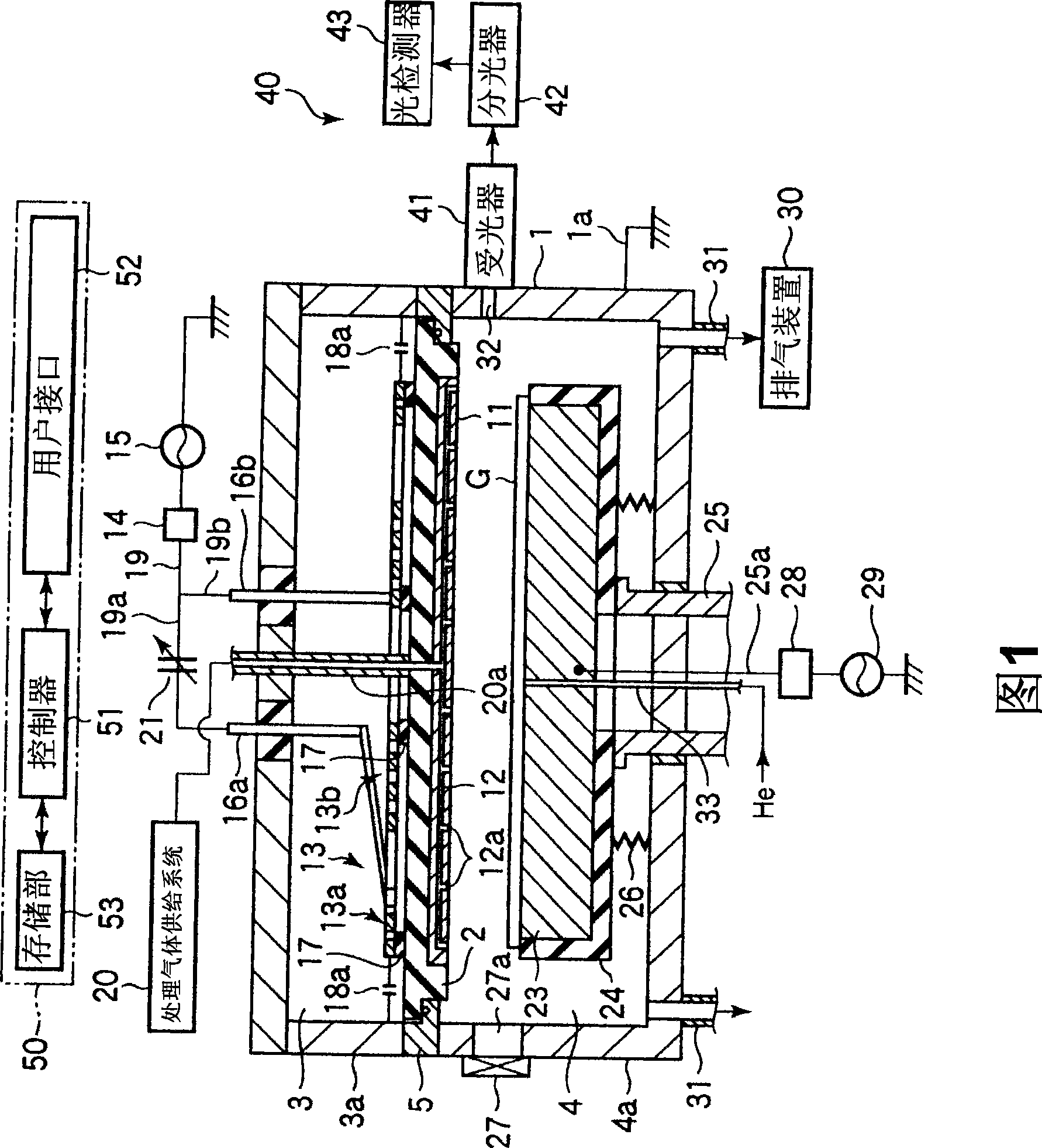
[0074] Hereinafter, embodiments of the present invention will be described with reference to the drawings. FIG. 1 is a cross-sectional view showing an inductively coupled plasma processing apparatus according to an embodiment of the present invention. figure 2 It is a plan view showing a high-frequency antenna used in this inductively coupled plasma processing apparatus. This apparatus is used, for example, for etching of metal films, ITO films, oxide films, etc., and ashing treatment of resist films when forming thin film transistors on a glass substrate for FPD. Here, as the FPD, a liquid crystal display (LCD), an electroluminescence (EL) display, a plasma display panel (PDP), etc. are exemplified.
[0075] This plasma processing apparatus has an airtight main body container 1 of a rectangular tube shape made of a conductive material such as aluminum whose inner wall surface is anodized. The main body container 1 is assembled in a disassembleable manner, and is grounded through...
PUM
 Abstract
Description
Claims
Application Information