Method for manufacturing copper conductor with improvable quality

A manufacturing method and technology of copper wires, which are applied in semiconductor/solid-state device manufacturing, electrical components, circuits, etc., can solve problems such as increasing the resistance value of copper wires, disconnection of metal wires, and easy gaps in copper wires, etc., so as to improve quality , to avoid the effect of the gap

Inactive Publication Date: 2009-05-27
SEMICON MFG INT (SHANGHAI) CORP
View PDF0 Cites 1 Cited by
  • Summary
  • Abstract
  • Description
  • Claims
  • Application Information

AI Technical Summary

Problems solved by technology

[0003] However, gaps are prone to appear on the copper wire made by the above-mentioned manufacturing method, and these gaps

Method used


Image

  • Method for manufacturing copper conductor with improvable quality

Examples


Embodiment Construction

[0015] The quality-improving copper wire manufacturing method of the present invention will be further described in detail below.

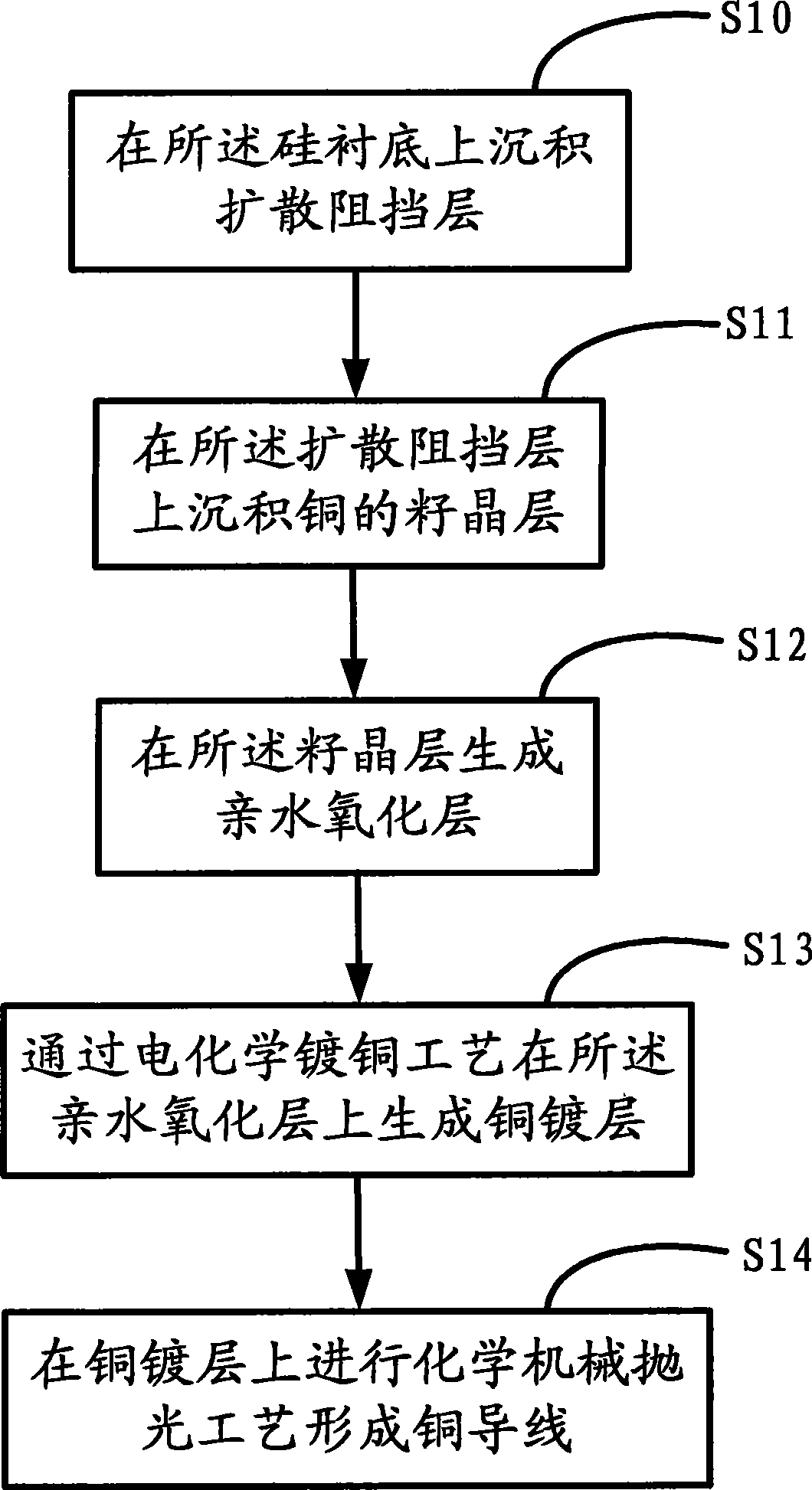
[0016] The quality-improving copper wire manufacturing method of the present invention is used for manufacturing copper wires on a silicon substrate, and the silicon substrate has grooves (may also include contact holes) for accommodating the copper wires. see figure 1 , the copper wire manufacturing method that can improve the quality of the present invention first carries out step S10, deposits the diffusion barrier layer on described silicon substrate, wherein, described diffusion barrier layer is the tantalum nitride layer (TaN) and tantalum layer stacked up and down (Ta) or a titanium nitride (TiN) layer and a titanium layer (Ti) stacked up and down. In this embodiment, the diffusion barrier layer is a tantalum nitride layer and a tantalum layer stacked up and down, which are deposited by atomic layer deposition (ALD). in the deposition mac...


PUM

PropertyMeasurementUnit
Thicknessaaaaaaaaaa

Abstract

The invention provides a copper conductor manufacturing method capable of improving quality, which is used for manufacturing a copper conductor on a silicon substrate. The prior art carries out a copper electrochemical plating process on an seed layer directly and part of the seed layer can not be plated with copper due to the poorer hydrophilic performance of the seed layer, so the manufactured copper conductor has notches and the quality of the copper conductor is seriously affected. The copper conductor manufacturing method capable of improving quality comprises the following steps: firstly, depositing a diffusion barrier layer on the silicon substrate; secondly, depositing a copper seed layer on the diffusion barrier layer; thirdly, generating a hydrophilic oxide layer on the seed layer; fourthly, generating a copper plating layer on the hydrophilic oxide layer through a copper electrochemical plating process; and finally, carrying out a chemical and mechanical polishing process on the copper plating layer to make the copper conductor. The method can avoid that part of the seed layer is not plated with copper to cause the notches on the copper conductor, and can greatly improve the quality of the copper conductor.

Description

technical field [0001] The invention relates to a metal wire manufacturing process, in particular to a copper wire manufacturing method capable of improving quality. Background technique [0002] With the continuous reduction of the minimum feature size (CD) of semiconductor devices (from the initial 1 mm to the current 90 nanometers or 60 nanometers, and will enter the era of 45 nanometers and 22 nanometers in the next few years), metal The current density in the wire is increasing and the response time is shortening. The traditional aluminum wire can no longer meet the needs of CD shrinking. Copper wire has gradually become the mainstream process in the semiconductor industry because of its lower resistivity and higher anti-electromigration ability than aluminum wire. The manufacturing method of the copper wire mainly includes the step of depositing a diffusion barrier layer, the step of depositing a copper seed layer, the step of electrochemical copper plating and the st...

Claims


Application Information

Patent Timeline
IPC IPC(8): H01L21/768
Inventor 聂佳相
Owner SEMICON MFG INT (SHANGHAI) CORP
Why Eureka
Try Eureka