Alignment light source apparatus

A technology of light source device and alignment mark, which is applied in the direction of exposure device, optics and optical components of photoengraving process, can solve the problems of stray light generated by integrated circuit graphics, high requirements of signal amplification system, and reduced signal-to-noise ratio, etc. Improve the utilization rate of laser light energy, reduce the laser spot, and reduce the effect of stray light

Active Publication Date: 2009-06-03
SHANGHAI MICRO ELECTRONICS EQUIP (GRP) CO LTD
View PDF1 Cites 16 Cited by
  • Summary
  • Abstract
  • Description
  • Claims
  • Application Information

AI Technical Summary

Problems solved by technology

[0007] In this technology, since the mark is long and the laser spot is circular, most of the energy is wasted when the light is irradiated on the quasi-mark, such as image 3 (a), (b) shown
Since the subsequent alignment signal processing is performed on the li

Method used


Image

  • Alignment light source apparatus
  • Alignment light source apparatus
  • Alignment light source apparatus

Examples


Example Embodiment

[0039] The specific embodiments of the present invention will be further described below in conjunction with the accompanying drawings.

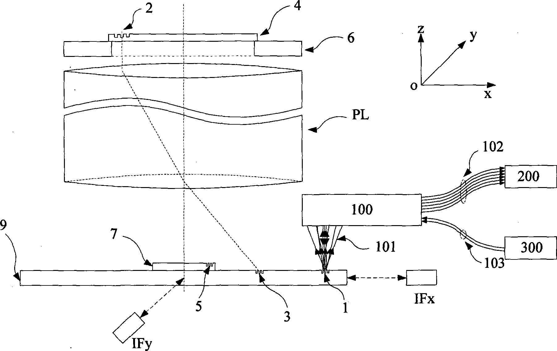
[0040] An alignment light source device of the present invention is used in a lithography alignment system, please refer to figure 1 , figure 1 Schematic diagram of the alignment system for the lithography equipment. The main structure includes: an alignment light source device 300 , an optical module 100 , alignment marks 1 , 2 , 3 , 5 , and a signal processing module 200 . Peripheral components include: mask plate 4 , mask stage 6 , projection objective lens PL, substrate 7 , substrate stage 9 , and transmission fibers 102 and 103 . The composition and functions of each structural module are described below.

[0041] The optical module 100 mainly includes a 4f system, an aperture, a reference grating, an optical path turning prism, and a detection fiber. Among them, the 4f system is mainly used to coherently image the diffracted ligh...


PUM


Abstract

The invention provides an alignment light source apparatus which comprises at least two sets of laser units having different wavelengths, wherein, the laser unit comprises a laser, a light intensity modulator, a phase modulator and a transmission fiber. The light path of a light beam is provided with a beam shaping device which comprises a first and a second optical rotation sheets, a first and a second polarizing beam splitters, a first and a second reshapers and a first and a second reflecting mirrors. The alignment light source apparatus reduces laser facula, improves the luminous energy utilization rate of the laser irradiated on the alignment mark and the intensity of alignment signals, increases the signal-to-noise of the alignment signals, and is beneficial to improving the alignment accuracy.

Description

technical field [0001] The invention relates to the field of integrated circuit manufacturing devices, and in particular to an alignment light source device and an alignment system used in photolithography equipment. Background technique [0002] Photolithography equipment is mainly used in the manufacture of integrated circuits IC or other micro devices. With a photolithographic apparatus, multilayer masks with different mask patterns are sequentially imaged in precise alignment on a photoresist-coated wafer, such as a semiconductor wafer or an LCD panel. Lithography devices are generally divided into two categories, one is a stepping lithography device, the mask pattern is exposed and imaged on one exposure area of ​​the wafer, and then the wafer moves relative to the mask to move the next exposure area to the mask pattern and under the projection objective, the mask pattern is again exposed on another exposed area of ​​the wafer, and the process is repeated until all exp...

Claims


Application Information

Patent Timeline
IPC IPC(8): G03F7/20G03F9/00G02B27/09G02B1/10
Inventor 王诗华徐荣伟
Owner SHANGHAI MICRO ELECTRONICS EQUIP (GRP) CO LTD
Why Eureka
Try Eureka