Delay grade selective circuit and correlation method thereof

A technology for selecting circuits and delay stages, applied to electrical components, pulse processing, generating/distributing signals, etc., can solve problems such as system operation errors

Active Publication Date: 2009-06-10
REALTEK SEMICON CORP
0 Cites 1 Cited by

AI-Extracted Technical Summary

Problems solved by technology

Ideally, after the required delay signal is determined, it can always meet the needs of the system and does not need to be changed. However, in practice, the d...

Method used

[0057] According to the above system and method, the delay amount can be changed in real time ...

Abstract

The invention relates to a delay-level selecting circuit, which comprises a first register for generating a plurality of sampling values according to a clock signal and a delay clock signal; a first storage unit for storing the sampling values and outputting the sampling values according to a first selecting signal; a selecting unit for outputting the sampling values according to a second selecting signal; a judging module for judging whether two continuous sampling values accord with a specific relation, deciding the specific delay level if the two continuous sampling values accord with the specific relation, and deciding the specific delay level according to a first count value; a counter for generating the count value to control the delay clock signal sampled by the first register; a first selecting signal generating circuit for generating the first selecting signal according to the count value; and a second selecting signal generating circuit for generating the second selecting signal according to the count value.

Application Domain

Single output arrangementsGenerating/distributing signals

Technology Topic

Numeric ValueClock signal +4

Image

  • Delay grade selective circuit and correlation method thereof
  • Delay grade selective circuit and correlation method thereof
  • Delay grade selective circuit and correlation method thereof

Examples

  • Experimental program(1)

Example Embodiment

[0031] Certain words are used in the description and claims to refer to specific components. Those skilled in the art should understand that hardware manufacturers may use different terms to refer to the same component. This specification and claims do not use differences in names as a way of distinguishing components, but use differences in functions of components as a criterion for distinguishing. The "include" mentioned in the entire specification and claims is an open term, so it should be interpreted as "include but not limited to". In addition, the term "coupled" herein includes any direct and indirect electrical connection means. Therefore, if it is described that a first device is coupled to a second device, it means that the first device can be directly electrically connected to the second device, or indirectly electrically connected to the second device through other devices or connecting means.
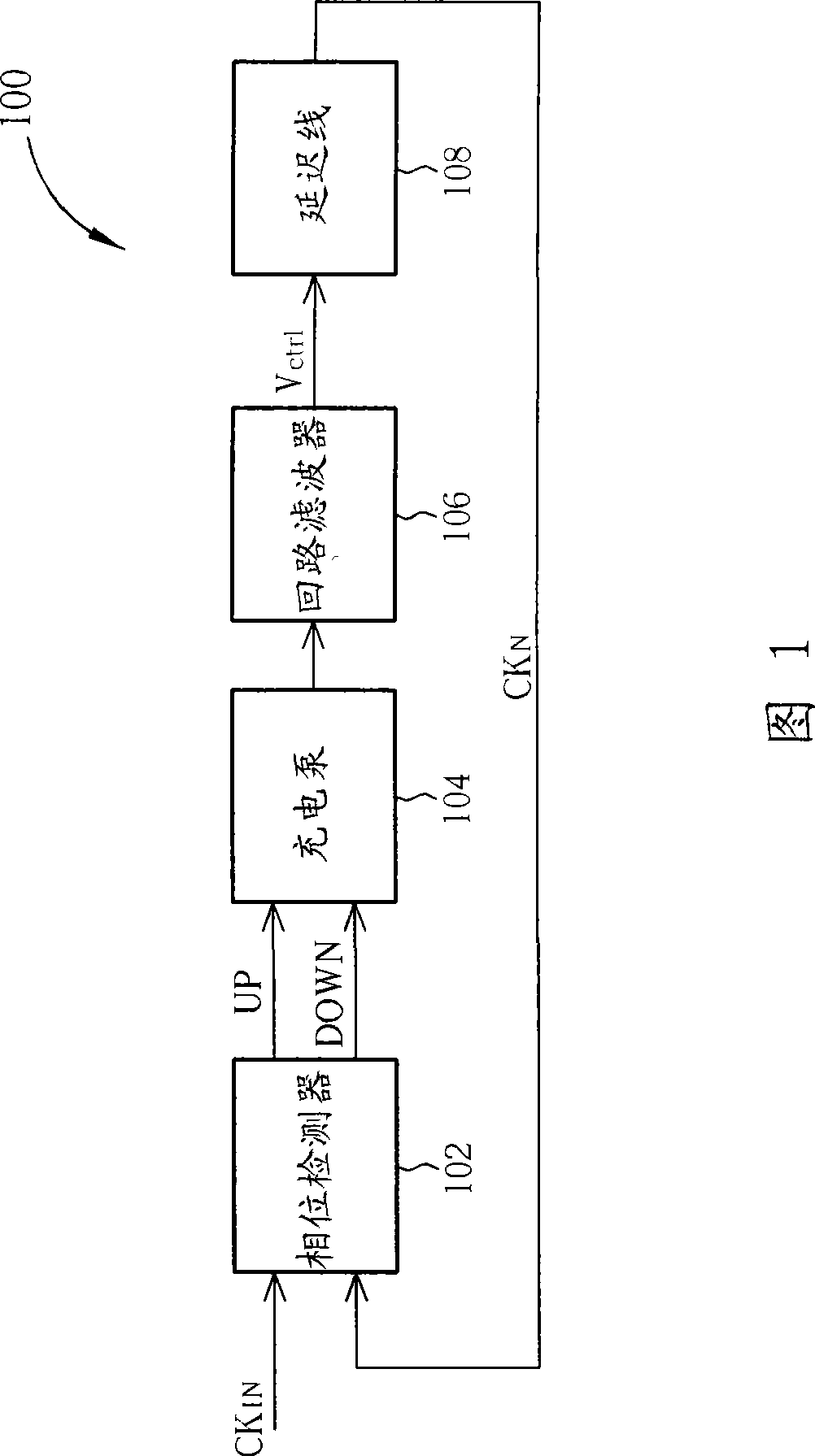
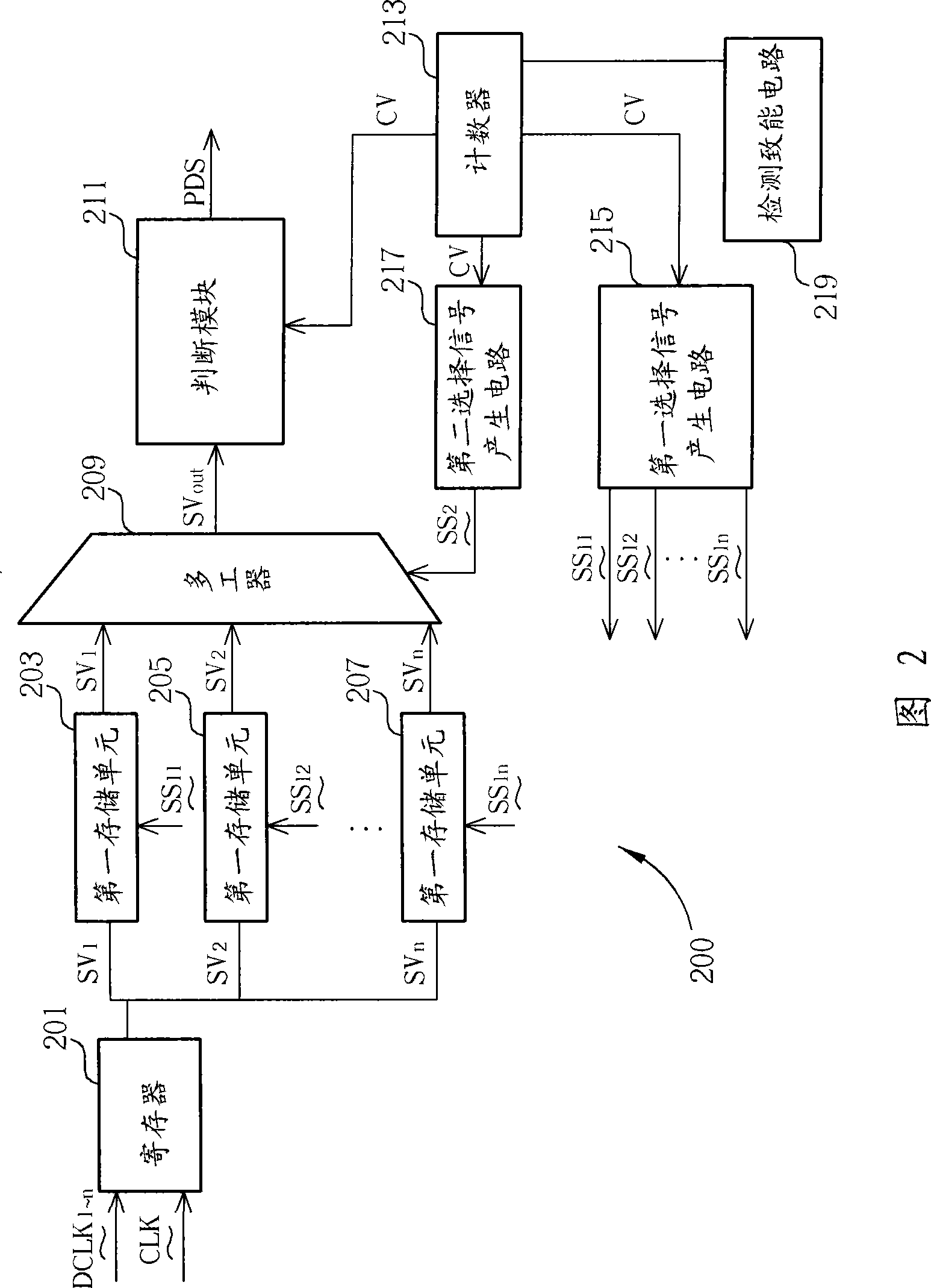
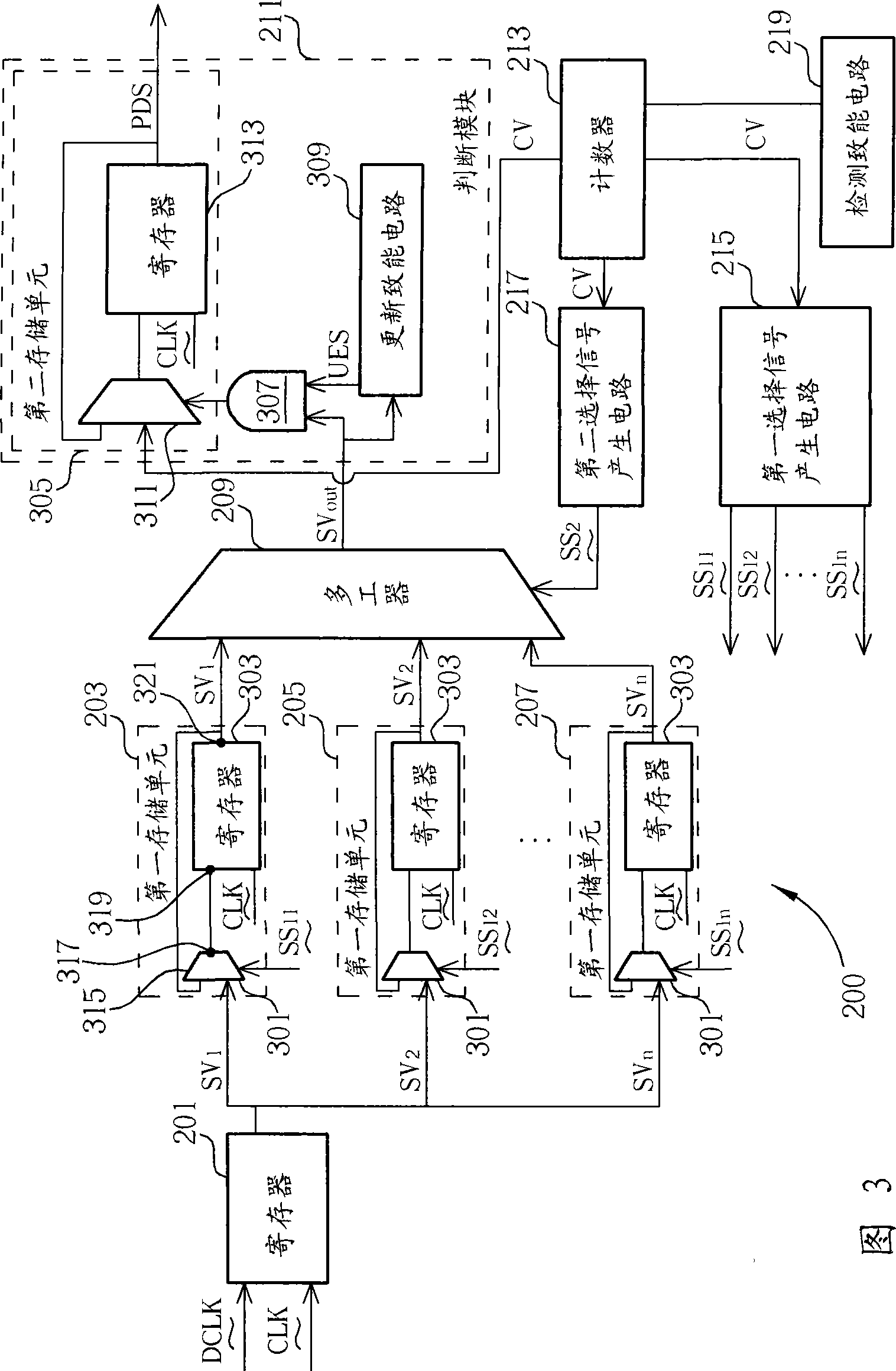
[0032] FIG. 2 shows a delay stage selection circuit 200 according to an embodiment of the present invention. As shown in FIG. 2, the delay stage selection circuit 200 is used to select a specific delay stage from a plurality of delay stages. In short, it generates a specific delay stage parameter PDS so that subsequent circuits select according to the specific delay stage parameter PDS Corresponding delay stages, these delay stages respectively output multiple delayed clock signals. The delay stage selection circuit 200 includes a register 201, a plurality of first storage units 203, 205, 207, a multiplexer 209, a judgment module 211, a counter 213, a first selection signal generation circuit 215, and a second Select signal generating circuit 217. It should be noted that only three first storage units are shown in this example, but it is not intended to limit the present invention. The register 201 is coupled to a plurality of delay stages (not shown) for respectively sampling a plurality of delayed clock signals DCLK according to a clock signal CLK 1-n To generate multiple sample values ​​SV 1 , SV 2...SV n. The first storage units 203, 205, and 207 are coupled to the first register 201, and respectively store the sample value SV 1 , SV 2...SV n , And respectively according to the corresponding first selection signal SS 11 , SS 12...SS 1n Output sample value SV 1 , SV 2...SV n. The multiplexer 209 is coupled to the first storage units 203, 205, and 207, and is configured to respond to a second selection signal SS 2 Separately output the sampled value SV 1 , SV 2...SV n One of them is the output value SV out.
[0033] The judging module 211 is coupled to the multiplexer 209 for judging the self-sampled value SV of the multiplexer 209 1 , SV 2...SV n Whether the two consecutive sampled values ​​selected in the selection match a specific relationship, and when the two consecutive sampled values ​​(for example, SV 4 And SV 5 ) When a specific relationship is met, based on the second sampled value (in this example, SV 5) And the count value CV generated by the counter 213 to determine the specific delay level. The counter 213 is coupled to the judgment module 211 for generating a count value CV to control a delayed clock signal sampled by the register 201. In detail, when the count value CV is 1, the register 201 uses the clock signal CLK to sample the delayed clock signal DCLK generated by the first delay stage. 1 When the count value CV is 2, the register 201 uses the clock signal CLK to sample the delayed clock signal DCLK generated by the first delay stage 2...And so on. The first selection signal generating circuit 215 is coupled to the counter 213 to generate a plurality of first selection signals SS according to the count value CV 11 , SS 12...SS 1n. First selection signal SS 11 , SS 12...SS 1n It is used to determine whether the count value CV will be output to the multiplexer 209. The second selection signal generating circuit 217 is coupled to the multiplexer 209 and the counter 213 for setting the second selection signal SS according to the count value CV 2. Second selection signal SS 2 Used to determine the sampling value SV 1 , SV 2...SV n Whether it will be output to the judging module 211. In this embodiment, the specific relationships stored in the first storage units 203, 205, and 207 are all 0 or 1, and when the first of the two consecutive count values ​​is 0 and the second is 1 (that is, the aforementioned Specific relationship), the second selection signal SS 2 So that the multiplexer will output the output value SV with a value of 1. out To the judgment module 211, when the judgment module 211 receives 1, it outputs the specific delay level parameter PDS. Then the subsequent system or circuit can use the specific delay level parameter PDS to re-determine a new delay level. Since how to select a new delay level according to the specific delay level parameter PDS is known to those skilled in the art, it will not be repeated here. It should be noted that this concept is not limited to when the first of two consecutive count values ​​is 0 and the second is 1, it can also be when the first of two consecutive count values ​​is 1 and the second It can be determined according to different sampling methods and circuits, and it does not depart from the scope of the present invention. In addition, in this embodiment, the clock signal CLK can be shared with other circuits, and the predetermined delay stage is selected so that the phase difference between the delayed clock signal DCLK and the clock signal CLK is 1/2 cycle of the clock signal CLK, but it is not used for Limit the present invention.
[0034] In summary, when the count value CV is 1, the register 201 samples DCLK 1 And the first storage unit 203 stores the sampled value SV 1 , When the count value is 2, the register 201 samples DCLK 2 And the first storage unit 205 stores the sample value SV 2......When the count value is n, register 201 samples DCLK n And the n-th first storage unit 207 stores the sample value SV n. The values ​​stored in the first storage units 203, 205, and 207 are also output according to the count value CV. For example, when the count value is 1, SS 11 Make the value of the first storage unit 203 output, when the count value is 2, SS 12 Make the value of the first storage unit 205 output, when the count value is n, SS 1n The value of the first storage unit 207 is output. When the count value is 1, SS 2 Make the multiplexer output the sampled value SV 1 And become the output value SV out , When the count value is 2, SS 2 Make the multiplexer output the sampled value SV 2 And become the output value SV out......When the count value is n, SS 2 Make the multiplexer output the sampled value SV n And become the output value SV out. Therefore, when the sampled value S 11 -S 1n. When the first situation is changed from 0 to 1 (meaning that the first 1 appears), the judgment module 211 receives the output value SV with a value of 1. out , And output the current count value CV as a specific delay level parameter PDS. For example, suppose the sample value SV is stored 1 , SV 2 And SV 3 Is 0, and the sampled value SV is stored 4 When it is the first 1, the judgment logic 211 will output the current count value CV (4 in this example) as the value of the specific delay stage signal PDS, and the subsequent circuit will select the new value according to the value of the specific delay stage signal PDS. The basis of the delay level. In this embodiment, the value of the delay stage signal PDS is directly used as the order of the new delay stage (for example, if the value of the delay stage signal PDS is 4, the fourth delay stage is selected as the new delay stage), but it is not intended to limit this invention.
[0035] It should be noted that the count value CV and the first selection signal SS 11 , SS 12...SS 1n , The second selection signal SS2, and DCLK 1-n It is not necessarily the above-mentioned corresponding relationship, and the corresponding relationship may also be as shown below. For example, it does not work when the count value CV is 1-2. When the count value is 3, register 201 samples DCLK 1 And the first storage unit 203 stores the sampled value SV 1 , When the count value is 4, register 201 samples DCLK 2 And the first storage unit 205 stores the sample value SV 2......When the count value is n+2, register 201 samples DCLK n And the first storage unit 207 stores the sampled value SV n. When the count value is 3, SS 11 Make the value of the first storage unit 203 output, when the count value is 4, SS 12 When the value of the first storage unit 205 is output, and the count value is n+2, SS 1n The value of the first storage unit 207 is output. When the count value is 3, SS 2 Make the multiplexer output the sampled value SV 1 And become the output value SV out , When the count value is 4, SS 2 Make the multiplexer output the sampled value SV 2 And become the output value SV out......When the count value is n+2, SS 2 Make the multiplexer output the sampled value SV n And become the output value SV out. Therefore, when the sampled value SV 1 , SV 2...SV n When the first change from 0 to 1 occurs (or the first 1 appears), the judgment module 211 receives the output value SV with a value of 1. out , And output the current count value CV as a specific delay level parameter PDS. Therefore, the count value CV and the first selection signal SS 11 , SS 12...SS 1n , The second selection signal SS 2 , And DCLK 1-n It can be adjusted according to needs, and it does not depart from the scope of the present invention.
[0036] Based on the above examples, when a count value SV is generated, the corresponding selection signal will cause it to be output to the multiplexer 209 (for example, SV 1 When produced, SS 11 It will be output to the multiplexer 209). However, this operation method is only used as an example, and is not intended to limit the present invention. For example, all the count values ​​SV can be calculated first and stored in the first storage unit respectively, and then the first selection signal is used to output them respectively, which is also within the scope of the present invention. And the above multiplexer can also be replaced by other selection units with the same function.
[0037] The delay stage selection circuit 200 may further include a detection enabling circuit for enabling the counter 213 to count the count value CV, and after the determination module 211 determines a specific delay stage, the counter stops counting the count value CV.
[0038] FIG. 3 shows a delay stage selection circuit 200 according to an embodiment of the present invention. It should be noted that FIG. 3 is only used as an example, and is not intended to limit the present invention. Those skilled in the art can easily modify these structures to obtain the same result, which does not depart from the scope of the present invention. As shown in FIG. 3, each of the first storage units 203, 205, and 207 includes a multiplexer 301 and a second register 303. An input terminal of the multiplexer 301 is coupled to the register 201 to receive the sample value SV respectively 1 -SV n , And its other selection terminal respectively receives the first selection signal SS 11 -SS 1n. The clock terminal of the register 303 is coupled to the clock signal CLK, one output terminal 321 is coupled to an input terminal 315 of the multiplexer 301, and the other input terminal 319 is coupled to an output terminal 317 of the multiplexer 301, wherein The multiplexer 301 according to the first selection signal SS 11 -SS 1n Optionally couple the output terminal of the register 201 to the input terminal of the register 303 or the sampling value SV 1 -SV n Output to the data terminal of the register 303. In this example, if the first selection signal SS 11 , SS 12...SS 1n If the sampled value from register 201 is not output to the data terminal of register 303, the output of register 303 will always remain at the previous output. When the data terminal of register 303 is switched to the sampled value of register 201, register 303 will switch to Output sample value SV 1 -SV n.
[0039] The judgment module 211 may include a second storage unit 305, an AND gate 307, and an update enable circuit 309. The second storage unit 305 includes a multiplexer 311 and a register 313. The update enable circuit 309 is used to generate an update enable signal UES when two consecutive sampled values ​​meet the specific relationship. The AND gate 307 is coupled to the multiplexer 209 and the update enable circuit 309 for generating an output value according to the output of the multiplexer 209 and the update enable circuit 309. The second storage unit 305 is coupled to the AND gate 307 and the counter 213 for determining whether to use the original specific delay level parameter PDS or output the count value CV as the new specific delay level parameter PDS according to the output value of the AND gate 307 , Wherein when the update enabling circuit 309 is based on the sampled value SV 1 -SV n When the update enable signal UES is generated, the second storage unit 305 is updated with the count value corresponding to the second sampling value.
[0040] In the above example, when the sampling value SV 1 -SV n When changing from 0 to 1 for the first time, the output value SV outIt is 1 and is output to the AND gate 307 and the update enable circuit 309. At this time, the update enable 309 will also output a value of 1, so the output value of the AND gate 307 will also be 1. When the multiplexer 311 receives the value 1 as the selection signal, it switches its output to the count value CV, and then the register 313 uses the count value CV as the specific delay level parameter PDS. It should be noted that the AND gate 307 mentioned above can be replaced by other logic units as required, which is also within the scope of the present invention.
[0041] Figure 4 The delay stage selection method corresponding to the delay stage selection circuit 200 shown in FIG. 3 is shown. Such as Figure 4 As shown, this delay level selection method includes:
[0042] Step 401:
[0043] The delayed clock signal of the clock signal is sampled according to a clock signal to generate a plurality of sample values.
[0044] Step 403:
[0045] Each sample value is stored separately, and the sample value is output according to the corresponding first selection signal.
[0046] Step 405:
[0047] The sampled values ​​are respectively output according to a second selection signal.
[0048] Step 407:
[0049] It is determined whether two consecutive first and second sample values ​​in the sample value meet a specific relationship, and when the two consecutive first and second sample values ​​meet the specific relationship, a specific delay level is determined.
[0050] Step 409:
[0051] A count value is generated to control a delayed clock signal sampled in step 401.
[0052] Step 411:
[0053] The first selection signal is generated according to the count value.
[0054] Step 413:
[0055] The second selection signal is set according to the count value.
[0056] The other detailed steps of this method have been disclosed in the description of FIG. 2 and FIG. 3, so they will not be repeated here.
[0057] According to the above-mentioned system and method, the delay amount can be changed in real time according to different states, so various problems caused by wrong delay amount can be avoided.
[0058] The foregoing is only an embodiment of the present invention, and all equivalent changes and modifications made in accordance with the claims of the present invention should fall within the scope of the present invention.

PUM

no PUM

Description & Claims & Application Information

We can also present the details of the Description, Claims and Application information to help users get a comprehensive understanding of the technical details of the patent, such as background art, summary of invention, brief description of drawings, description of embodiments, and other original content. On the other hand, users can also determine the specific scope of protection of the technology through the list of claims; as well as understand the changes in the life cycle of the technology with the presentation of the patent timeline. Login to view more.
Why Eureka
Try Eureka