Circuit for buffering having a coupler

A buffer circuit and coupler technology, applied in logic circuits, logic circuit coupling/interfaces using field effect transistors, DC coupled DC amplifiers, etc., can solve the problem of slowing down the working speed of the buffering circuit and achieve the goal of improving the working speed Effect

Inactive Publication Date: 2009-06-10
SK HYNIX INC
View PDF0 Cites 2 Cited by
  • Summary
  • Abstract
  • Description
  • Claims
  • Application Information

AI Technical Summary

Problems solved by technology

In this case, the NMOS transistors N1, N2 limit the current flowing, which slows down the operation of the snubber circuit

Method used


Image

  • Circuit for buffering having a coupler
  • Circuit for buffering having a coupler
  • Circuit for buffering having a coupler

Examples


Embodiment Construction

[0025] Hereinafter, specific embodiments of the present invention will be described in detail with reference to the accompanying drawings.

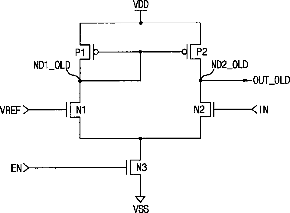
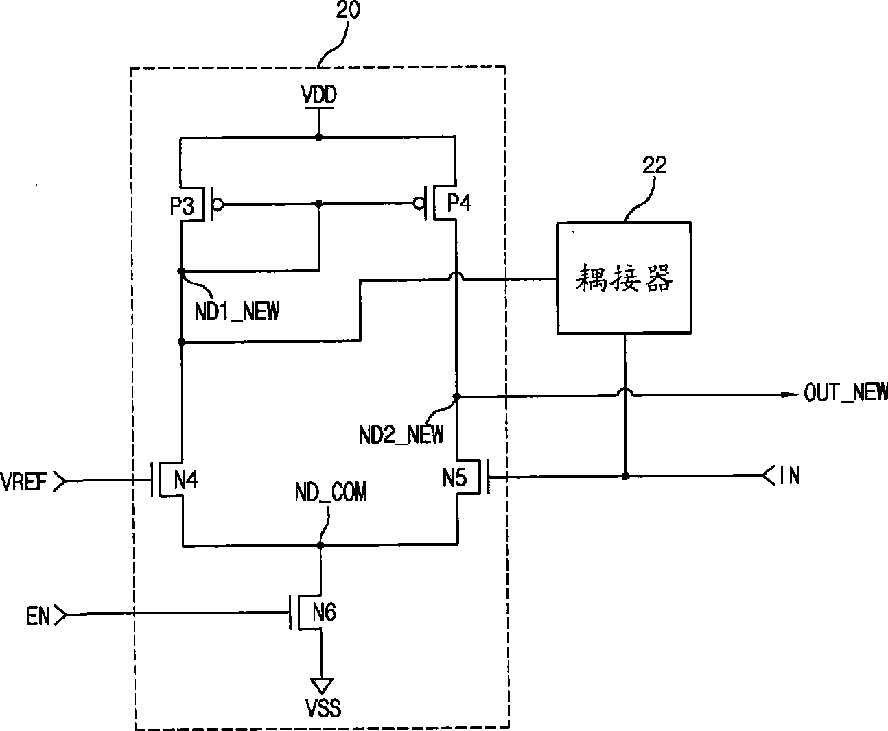
[0026] The invention discloses a buffer circuit with a coupler for controlling a bias for differential amplification by coupling an input signal with a reference node corresponding to a reference voltage.

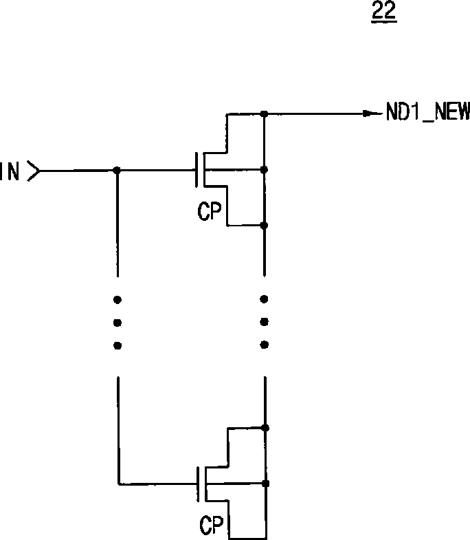
[0027] Specifically, the buffer circuit according to the present invention includes: a differential amplifier 20 for sensing and amplifying the potential difference between a reference voltage VREF and an input signal IN; and a coupler 22 for making the input signal IN and an input signal IN The reference node ND1_NEW corresponding to the reference voltage VREW is coupled, such as figure 2 shown.

[0028] The differential amplifier 20 differentially amplifies the reference node ND1_NEW and an input node ND2_NEW, and outputs an output signal OUT_NEW corresponding to the potential of the amplified input node ND2_NEW. The reference nod...


PUM


Abstract

The buffer circuit includes a differential amplifier differentially amplifying a reference node corresponding to a reference voltage and an input node corresponding to the input signal by sensing a potential difference of the reference voltage and the input signal. A coupling unit couples the input signal to the reference node, making it possible to improve the operating speed of the buffer circuit and operate normally when a level of the input signal or the reference voltage becomes low.

Description

technical field [0001] The present invention relates to a semiconductor device, and more particularly to a buffer circuit capable of buffering an input signal. Background technique [0002] Generally, a semiconductor device includes a buffer circuit that receives external signals (eg, data, addresses, commands, etc.) and converts the external signals into signals suitable for an internal logic. [0003] A conventional buffer circuit includes a differential amplifier that senses and amplifies the potential difference between a reference voltage VREF and an input signal IN, such as figure 1 shown. [0004] Specifically, two PMOS (P-type metal-oxide-semiconductor) transistors P1 and P2 are formed in a current mirror structure to supply the same current to the two nodes ND1_OLD and ND2_OLD, and are based on NMOS (N-type metal-oxide-semiconductor) The potential difference between the reference voltage VREF received by the transistor N1 and the input signal IN received by the NM...

Claims


Application Information

Patent Timeline
Patent Type & Authority Applications(China)
IPC IPC(8): H03K19/0175H03K19/0185H03F3/45
CPCH03K19/01721H03K19/018528H03K19/01707G11C7/062G11C7/10H03F3/45
Inventor 李种天
Owner SK HYNIX INC
Why Eureka
Try Eureka