Supercharge Your Innovation With Domain-Expert AI Agents!

Method for removing interconnecting metal layer surface oxidation membrane

A technology for interconnecting metals and surface oxidation, which is applied in the direction of electrical components, semiconductor/solid-state device manufacturing, circuits, etc. It can solve problems such as long time, rough surface morphology, and damage to the surface of the interconnected metal layer to avoid damage and reduce Effects of lattice changes

Inactive Publication Date: 2009-06-17
SEMICON MFG INT (SHANGHAI) CORP +1
View PDF1 Cites 8 Cited by
  • Summary
  • Abstract
  • Description
  • Claims
  • Application Information

AI Technical Summary

Problems solved by technology

At present, the method of removing the oxide film on the surface of the interconnected metal layer is plasma sputtering of an inert gas. The sputtering time depends on the thickness of the oxide film on the surface of the interconnected metal layer. The time for plasma sputtering to remove the oxide film on the surface of the interconnection metal layer is relatively long. Long-term continuous plasma sputtering will damage the surface of the interconnection metal layer, resulting in the subsequent formation of the under-bump metal layer and the cross-section and thickness of the bump. rough surface

Method used


Image

  • Method for removing interconnecting metal layer surface oxidation membrane
  • Method for removing interconnecting metal layer surface oxidation membrane
  • Method for removing interconnecting metal layer surface oxidation membrane

Examples


Embodiment

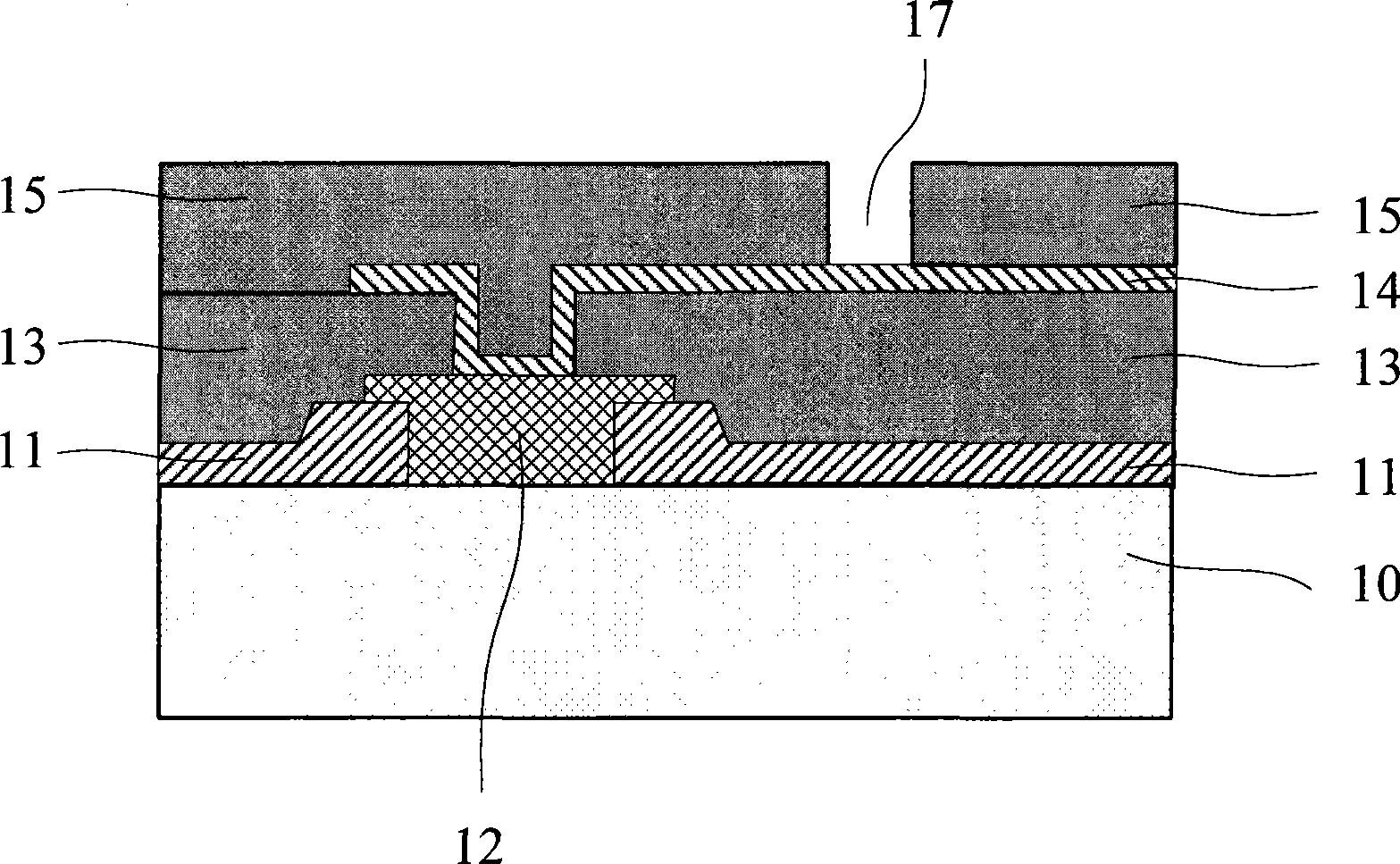
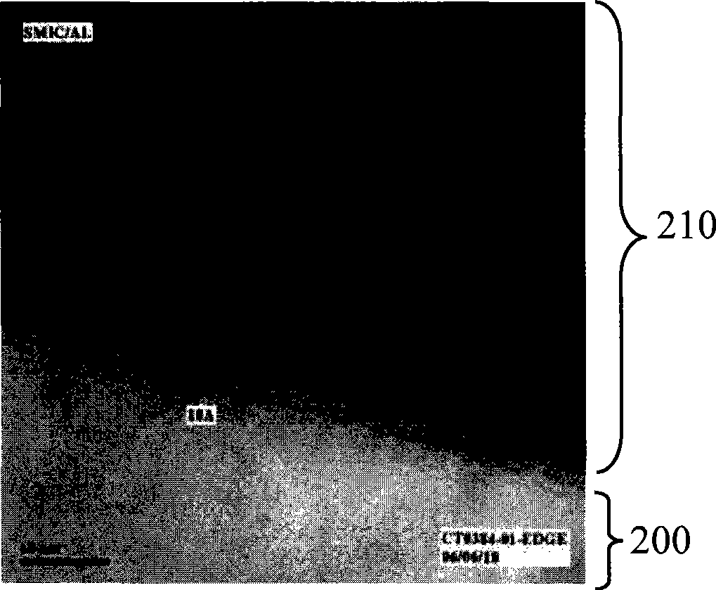
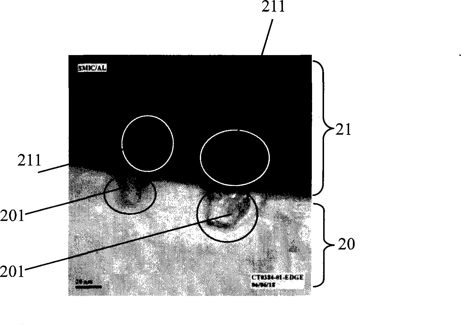
[0031] as attached figure 1 In the structure of the redistributed bumps shown, the material of the interconnected metal layer is metal aluminum. Since metal aluminum is extremely easy to oxidize in the air, an oxide film is formed. Therefore, as an example, ensure that the interconnected metal layer and the formed on The good electrical connection relationship of the redistributed metal layer needs to remove the oxide film layer on the surface of the interconnected metal layer. At present, the commonly used method for removing the oxide film layer is to use plasma sputtering, through non-oxidative plasma sputtering The surface of the interconnected metal layer is irradiated to achieve the purpose of removing the oxide film on the surface of the interconnected metal layer.

[0032] However, the time of plasma sputtering depends on the thickness of the oxide film on the surface of the interconnected metal layer. If the thickness of the oxide film is larger, the time of plasma sp...


PUM


Abstract

A method for removing an oxide film on the surface of an interconnection metal layer utilizes plasma of non-oxidizing gas to sputter for the oxide film on the surface of the interconnection metal layer, wherein the temperature of a reaction cavity is maintained lower than 23 DEG C during the sputtering process. In the technical scheme, a mild condition of plasma sputtering etching is provided, temperatures of the reaction cavity and the wafer surface can be controlled uniformly and freely, thereby reducing crystal lattice changes of the wafer surface caused by over high temperature, and avoiding damages to the surface of the interconnection metal layer when sputtering for the interconnection metal layer continuously in the prior art.

Description

technical field [0001] The invention relates to the technical field of semiconductor manufacturing, in particular to a method for removing an oxide film on the surface of an interconnected metal layer. Background technique [0002] Wafer Level Chip Scale Package (WLCSP) is a CSP packaging technology that enables integrated circuits (ICs) to be mounted face-down on printed circuit boards. The solder joints of the wafer pass through independent bumps such as solder balls. Soldered to the interconnect metal layer of the printed circuit board without any filler material. The first advantage of this technology is that the inductance between the integrated circuit and the printed circuit board is very small, and the second advantage is that the package size and production cycle are reduced and the heat conduction performance is improved. [0003] In wafer-level packaging, the distribution of connection points is denser. Therefore, it is necessary to redistribute the connection po...

Claims


Application Information

Patent Timeline
IPC IPC(8): H01L21/768
Inventor 章国伟梅娜王重阳江卢山
Owner SEMICON MFG INT (SHANGHAI) CORP
Features
  • R&D
  • Intellectual Property
  • Life Sciences
  • Materials
  • Tech Scout
  • Unparalleled Data Quality
  • Higher Quality Content
  • 60% Fewer Hallucinations
Learn More