Parasitic vertical PNP and manufacturing process thereof in BiCMOS process

A process, N-type technology, used in semiconductor/solid-state device manufacturing, electrical components, transistors, etc., can solve the problems of inability to meet chip integration requirements, low cut-off frequency, long transit time, etc., to eliminate adverse effects, improve Effect of Amplification Factor and Cutoff Frequency

Inactive Publication Date: 2009-06-17
SHANGHAI HUA HONG NEC ELECTRONICS
View PDF0 Cites 9 Cited by
  • Summary
  • Abstract
  • Description
  • Claims
  • Application Information

AI Technical Summary

Problems solved by technology

[0004] It can be seen that the traditional BiCMOS process includes CMOS, vertical NPN transistors, horizontal PNP transistors and some other capacitors, but due to the wide base width of the lateral PNP transi...

Method used


Image

  • Parasitic vertical PNP and manufacturing process thereof in BiCMOS process
  • Parasitic vertical PNP and manufacturing process thereof in BiCMOS process
  • Parasitic vertical PNP and manufacturing process thereof in BiCMOS process

Examples


Embodiment Construction

[0015] combine Figure 7 , the embodiment of the present invention includes the following steps:

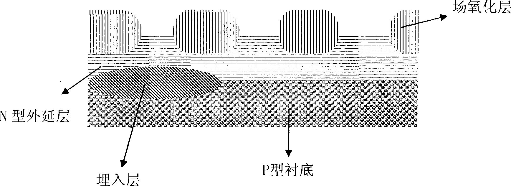
[0016] Such as figure 1 As shown, firstly, ion implantation of the buried layer is performed on the P-type substrate as the buried layer, N-type epitaxial growth and the formation of the active region.

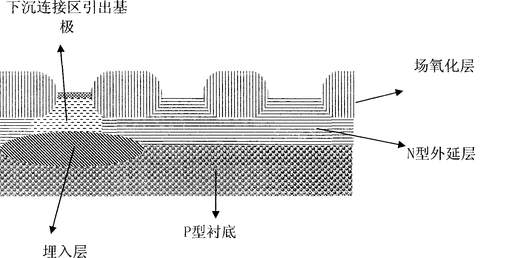
[0017] Secondly, if figure 2 As shown, ion implantation is carried out in the sinking connection layer. This layer is used as the vertical NPN collector and the parasitic lateral PNP base lead-out region in the BiCMOS process to connect with the outside world, and in the present invention as the base lead-out region of the vertical PNP.

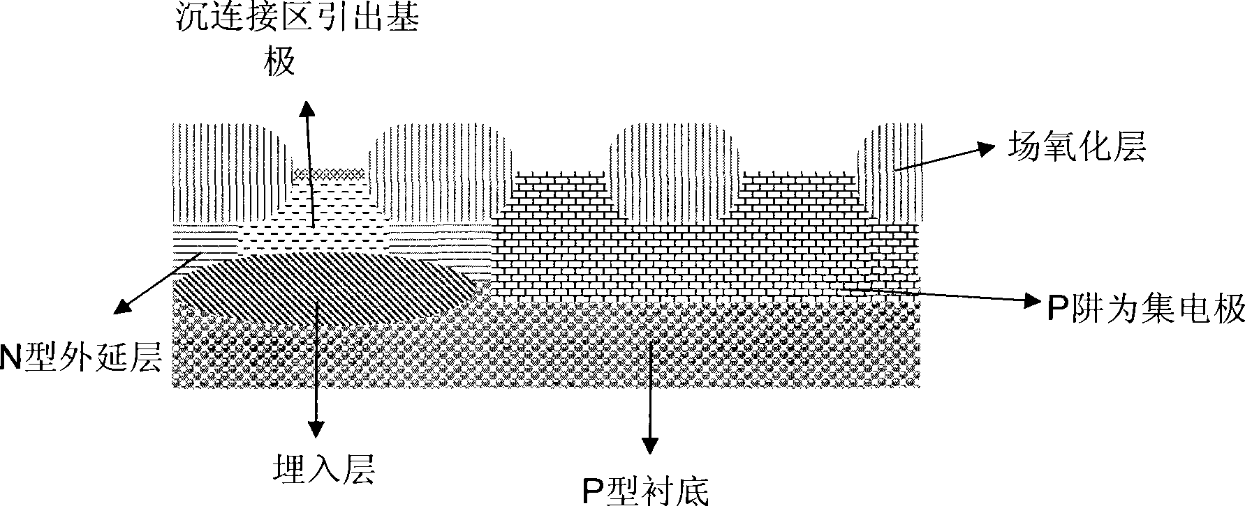
[0018] Then, if image 3 As shown, the CMOS P-well isolation ion implantation is performed while the vertical PNP region is opened for implantation, thereby forming a vertical PNP collector. The ion implantation depth penetrates the field oxide layer and the N-type epitaxial layer. At this time, the implanted ions are B, the energy is 400k...


PUM

PropertyMeasurementUnit
Thicknessaaaaaaaaaa

Abstract

The invention discloses a preparing method of a parasitic vertical PNP in the BiCMOS process, which comprises steps of 1, ion implantation of a buried layer, N type epitaxial growth and formation of an active region, 2, ion implantation of a subsided connection layer, 3, P-well isolating ion implantation of a CMOS, 4, N-well ion implantation of the CMOS, 5, forming a layer of oxide thin film through the oxidizing annealing treatment, growing base polysilicon and implanting boron as a P-type emitter, and finally etching away the base polysilicon in the non-vertical PNP region. The invention further discloses a parasitic vertical PNP in the BiCMOS process, which utilizes the P-well isolating ion implantation to form a collector electrode, uses the N-well reverse-punch ion implantation to form a base electrode, and utilizes base polysilicon implanted with boron as an emitter. By adjusting the ion implantation conditions of the N-well and the P-well, the invention can prepare parasitic vertical PNP triodes without adding a photomask or other cost, thereby increasing amplifying coefficient and cutoff frequency.

Description

technical field [0001] The invention relates to a BiCMOS process in the field of semiconductor manufacturing, in particular to a parasitic vertical PNP tube in the BiCMOS process and a preparation method for the parasitic vertical PNP tube in the BiCMOS process. Background technique [0002] BiCMOS technology is a technology that combines bipolar transistors and CMOS semiconductor structures. It combines the advantages of these two technologies. It not only has the advantages of low energy consumption and high integration of CMOS, but also has the advantage of speed. As the scale of semiconductor devices becomes larger and larger, the performance requirements for large-scale and ultra-large-scale integrated circuits are higher and higher, and the requirements for BiCMOS devices are also higher and higher. [0003] The existing BiCMOS process forms CMOS, vertical NPN transistors and parasitic lateral PNP transistors respectively. The process flow includes: formation of buried...

Claims


Application Information

Patent Timeline
IPC IPC(8): H01L21/8228H01L27/082
Inventor 徐炯周正良
Owner SHANGHAI HUA HONG NEC ELECTRONICS
Why Eureka
Try Eureka